Semiconductor chip and method for forming conductive pillar
A technology of semiconductors and conductor pillars, which is applied in the field of forming conductor pillar bumps, and can solve problems such as damage, failure rate, and damaged electronic components
- Summary
- Abstract
- Description
- Claims
- Application Information
AI Technical Summary
Problems solved by technology
Method used
Image

Examples
Embodiment Construction
[0044] The making and using of exemplary embodiments are discussed in detail below. It should be appreciated, however, that the present disclosure presents numerous feasible inventive concepts that can be embodied in many specific situations. The embodiments discussed are for purposes of illustration only and are not intended to limit the invention.
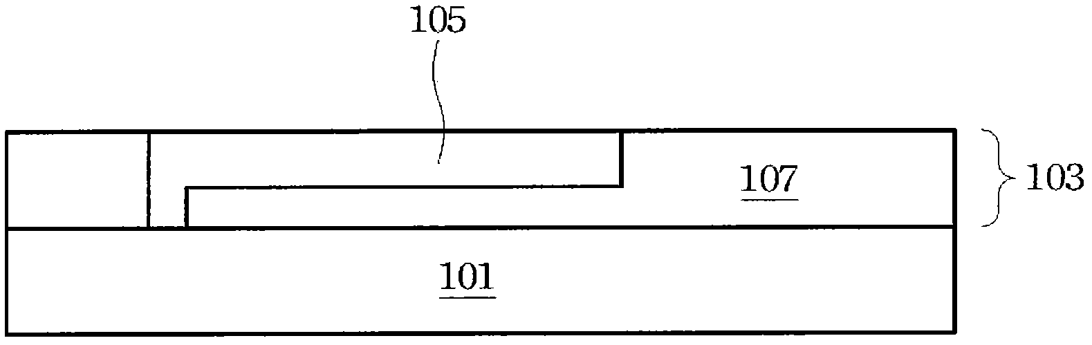
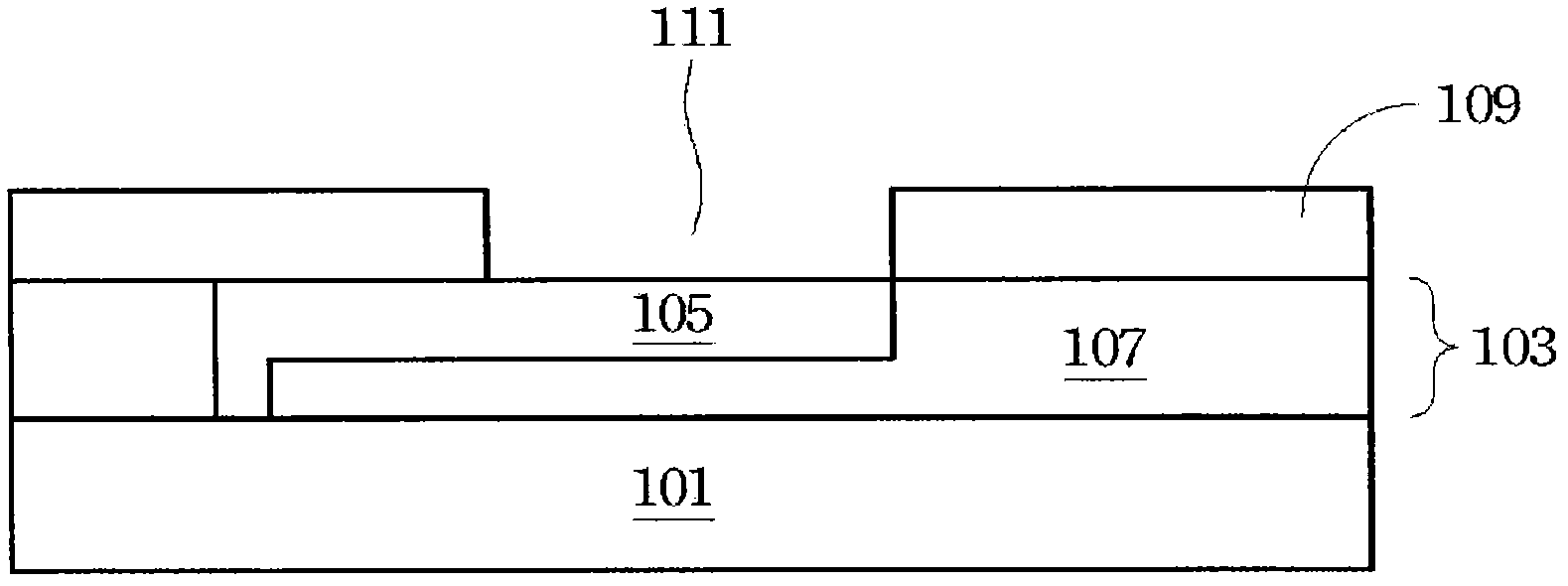
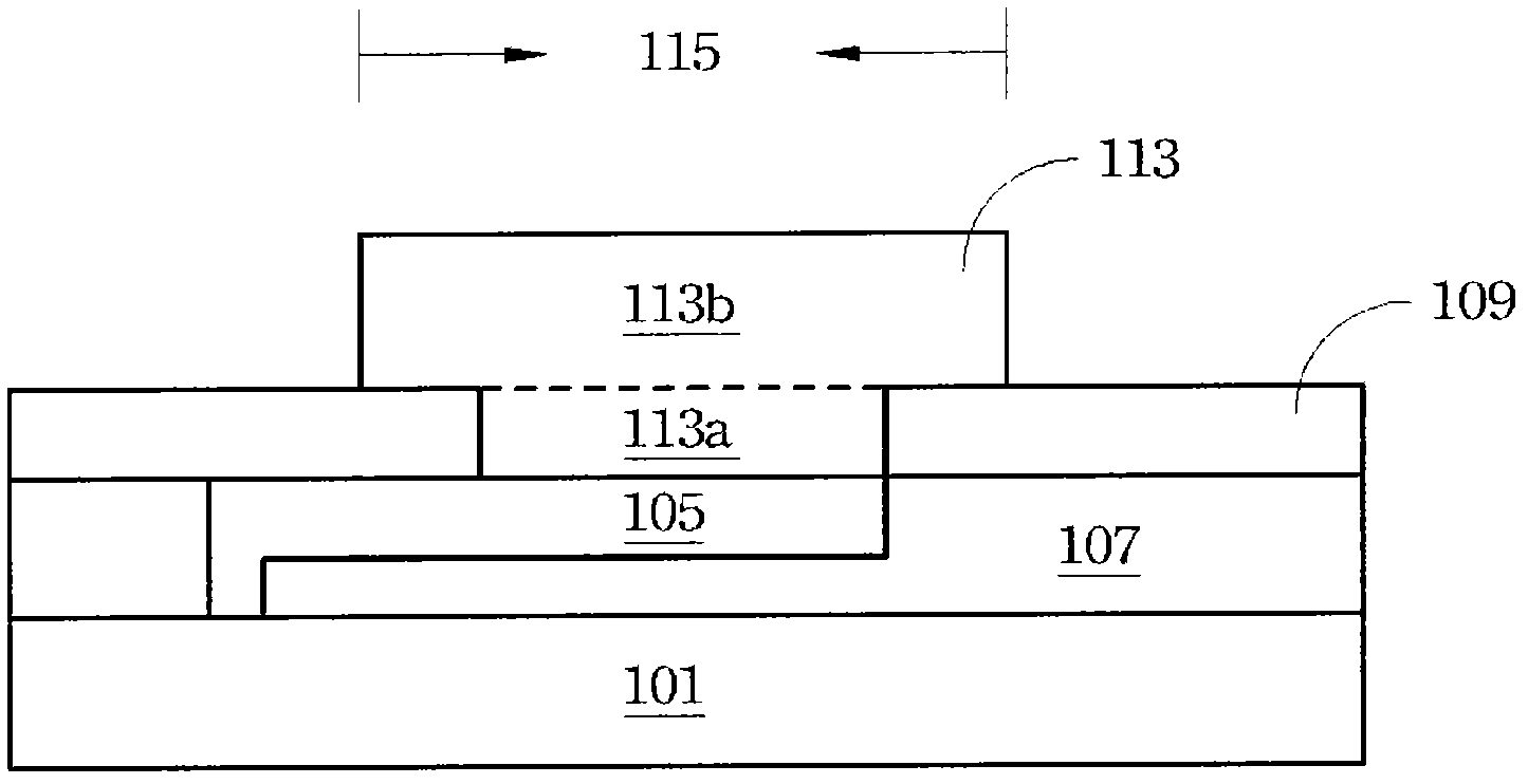
[0045] Figure 1 to Figure 7 are cross-sectional views of various stages of fabricating conductor posts on a substrate according to an embodiment of the present invention. Figure 8 A flow chart of a method 200 for fabricating conductor posts is shown. Where "substrate" generally refers to a semiconductor substrate on which various deposited layers and integrated circuits are formed. The substrate may comprise silicon or a compound semiconductor such as gallium arsenide (GaAs), indium phosphide (InP), silicon / germanium (Si / Ge), or silicon carbide (SiC). Examples of deposited layers include dielectric layers, doped layers, met...
PUM
 Abstract
Description
Claims
Application Information
 - R&D
- Intellectual Property
- Life Sciences
- Materials
- Tech Scout
- Unparalleled Data Quality
- Higher Quality Content
- 60% Fewer Hallucinations
Browse by: Latest US Patents, China's latest patents, Technical Efficacy Thesaurus, Application Domain, Technology Topic, Popular Technical Reports.
© 2025 PatSnap. All rights reserved.Legal|Privacy policy|Modern Slavery Act Transparency Statement|Sitemap|About US| Contact US: help@patsnap.com