ESD (electrostatic discharge) protection circuit
An ESD protection and circuit technology, applied in circuits, electrical components, electrical solid devices, etc., can solve problems such as poor electrostatic protection ability, and achieve the effect of increasing electrostatic protection, improving electrostatic protection, and improving performance.
- Summary
- Abstract
- Description
- Claims
- Application Information
AI Technical Summary
Problems solved by technology
Method used
Image
Examples
no. 1 example
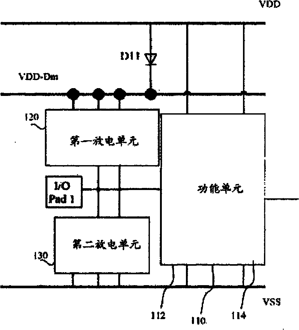
[0070] figure 2 It is a schematic diagram of the ESD protection circuit of the first embodiment of the present invention. Combine below figure 2 The ESD protection circuit of the first embodiment of the present invention is described, which mainly includes: a first power line VDD, a second power line VSS, a virtual power line VDD-Dm, a first input / output pad I / O pad1, a functional unit 110 , a first discharge unit 120 , a second discharge unit 130 , and a first cut-off diode D11 .
[0071] Wherein, the first end of the functional unit 110 is coupled to the first input / output pad I / O pad1; the second end of the functional unit 110 is coupled to the first power line VDD; the third end of the functional unit 11 is coupled to the first power line VDD. The second power line VSS is coupled.
[0072] The first terminal of the first discharge unit 120 is coupled to the first input / output pad I / O pad1 and the first terminal of the functional unit 110; the second terminal of the fi...
no. 2 example
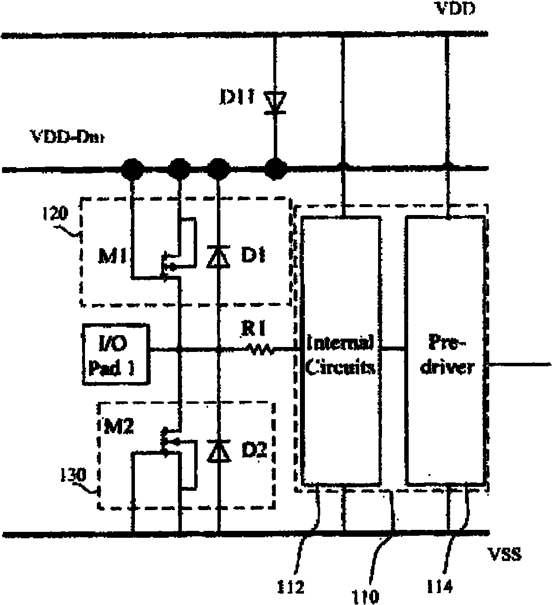
[0084] Figure 4 It is a schematic diagram of the ESD protection circuit of the second embodiment of the present invention. Combine below Figure 4 The ESD protection circuit of the second embodiment of the present invention is described, which mainly includes: a first power supply line VDD, a second power supply line VSS, a virtual power supply line VDD-Dm, a first input / output pad I / O pad1, a functional unit 110 , a first discharge unit 120 , a second discharge unit 130 , and a first cut-off diode D11 . Wherein, the first end of the functional unit 110 is coupled to the first input / output pad I / O pad1; the second end of the functional unit 110 is coupled to the first power line VDD; the third end of the functional unit 11 is coupled to the first power line VDD. The second power line VSS is coupled. The first terminal of the first discharge unit 120 is coupled to the first input / output pad I / O pad1 and the first terminal of the functional unit 110; the second terminal of t...
no. 3 example
[0115] Figure 5 It is a schematic diagram of the ESD protection circuit of the third embodiment of the present invention. Combine below Figure 5 The ESD protection circuit of the third embodiment of the present invention is described, which mainly includes: a first power supply line VDD, a second power supply line VSS, a virtual power supply line VDD-Dm, a first input / output pad I / O pad1, a functional unit 110 , a first discharge unit 120 , a second discharge unit 130 , and a first cut-off diode D11 . Wherein, the first terminal 1 of the functional unit 110 is coupled to the first input / output pad I / O pad1; the second terminal 2 of the functional unit 110 is coupled to the first power line VDD; the third terminal of the functional unit 11 3 is coupled to the second power line VSS. The first terminal of the first discharge unit 120 is coupled to the first input / output pad I / O pad1 and the first terminal 1 of the functional unit 110; the second terminal of the first dischar...
PUM
 Abstract
Description
Claims
Application Information
 - R&D Engineer
- R&D Manager
- IP Professional
- Industry Leading Data Capabilities
- Powerful AI technology
- Patent DNA Extraction
Browse by: Latest US Patents, China's latest patents, Technical Efficacy Thesaurus, Application Domain, Technology Topic, Popular Technical Reports.
© 2024 PatSnap. All rights reserved.Legal|Privacy policy|Modern Slavery Act Transparency Statement|Sitemap|About US| Contact US: help@patsnap.com


