Probe card and printed circuit board used for same

A printed circuit board and probe card technology, which is applied in the field of probe cards, can solve the problems of increasing overall cost expenditure, test error, noise interference, etc., and achieve the effects of good power integrity, cost saving and accuracy improvement

Active Publication Date: 2011-08-17
MICROELECTRONICS TECH INC
View PDF4 Cites 4 Cited by
  • Summary
  • Abstract
  • Description
  • Claims
  • Application Information

AI Technical Summary

Problems solved by technology

Since each power plane must use one or more layers for layout in the routing area, the power plane is prone to structural defects due to layer penetration, or the metal wires are densely distributed on the printed circuit board in order to avoid Through the signal solder joints of the printed circuit board, the wiring path of the metal wire is too complicated
Therefore, when the power input from the power pad passes through the power plane in the routing area, a voltage drop or noise interference often occurs, which will affect the integ

Method used


Image

  • Probe card and printed circuit board used for same
  • Probe card and printed circuit board used for same
  • Probe card and printed circuit board used for same

Examples


Embodiment Construction

[0024] In an embodiment of the probe card of the present invention, the power plane is separated from the printed circuit board, and the probes are supplied with power by means of an external power plane or direct wire connection. Relevant detailed description and technical contents of the present invention, now cooperate with accompanying drawing to illustrate as follows:

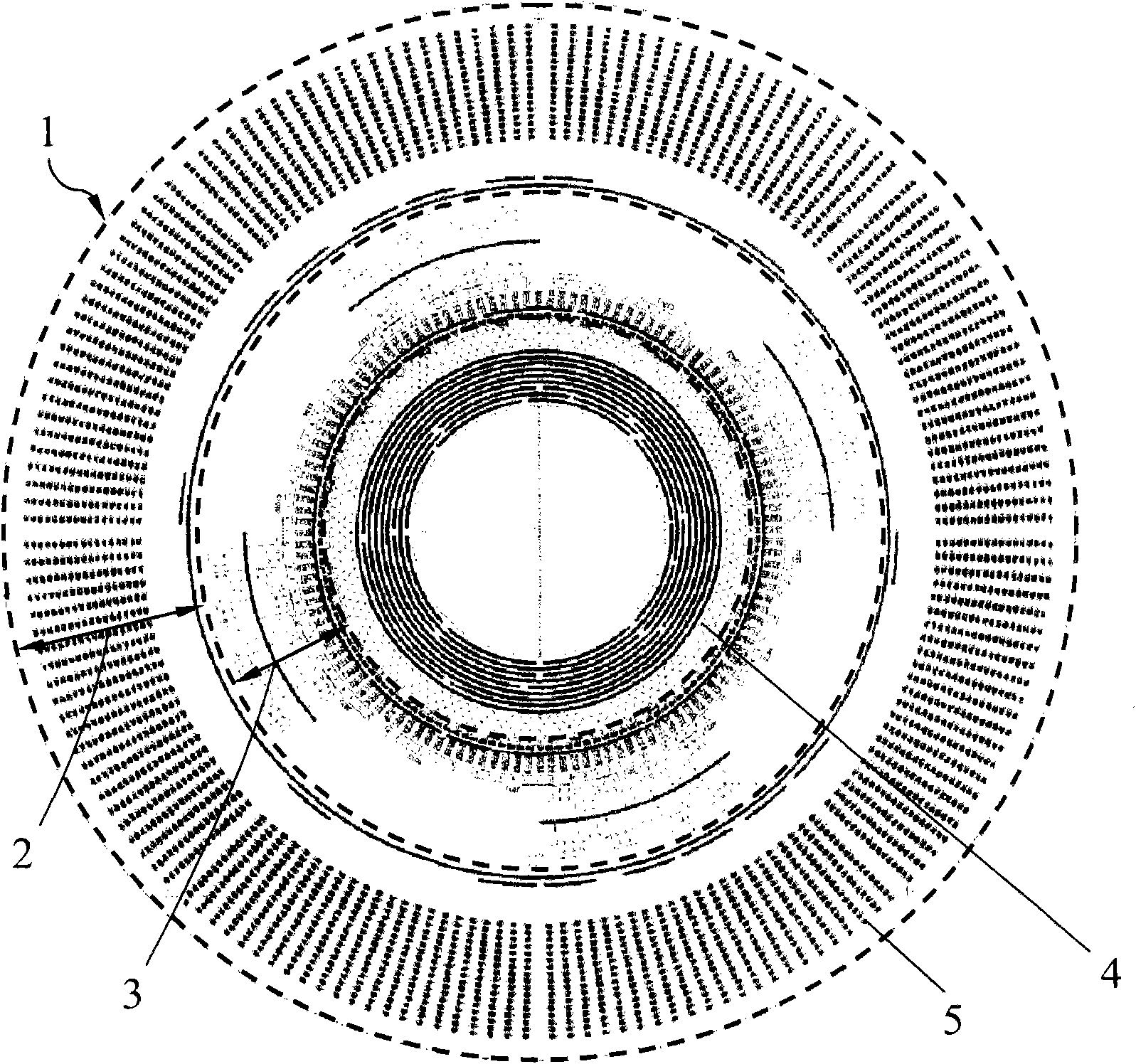
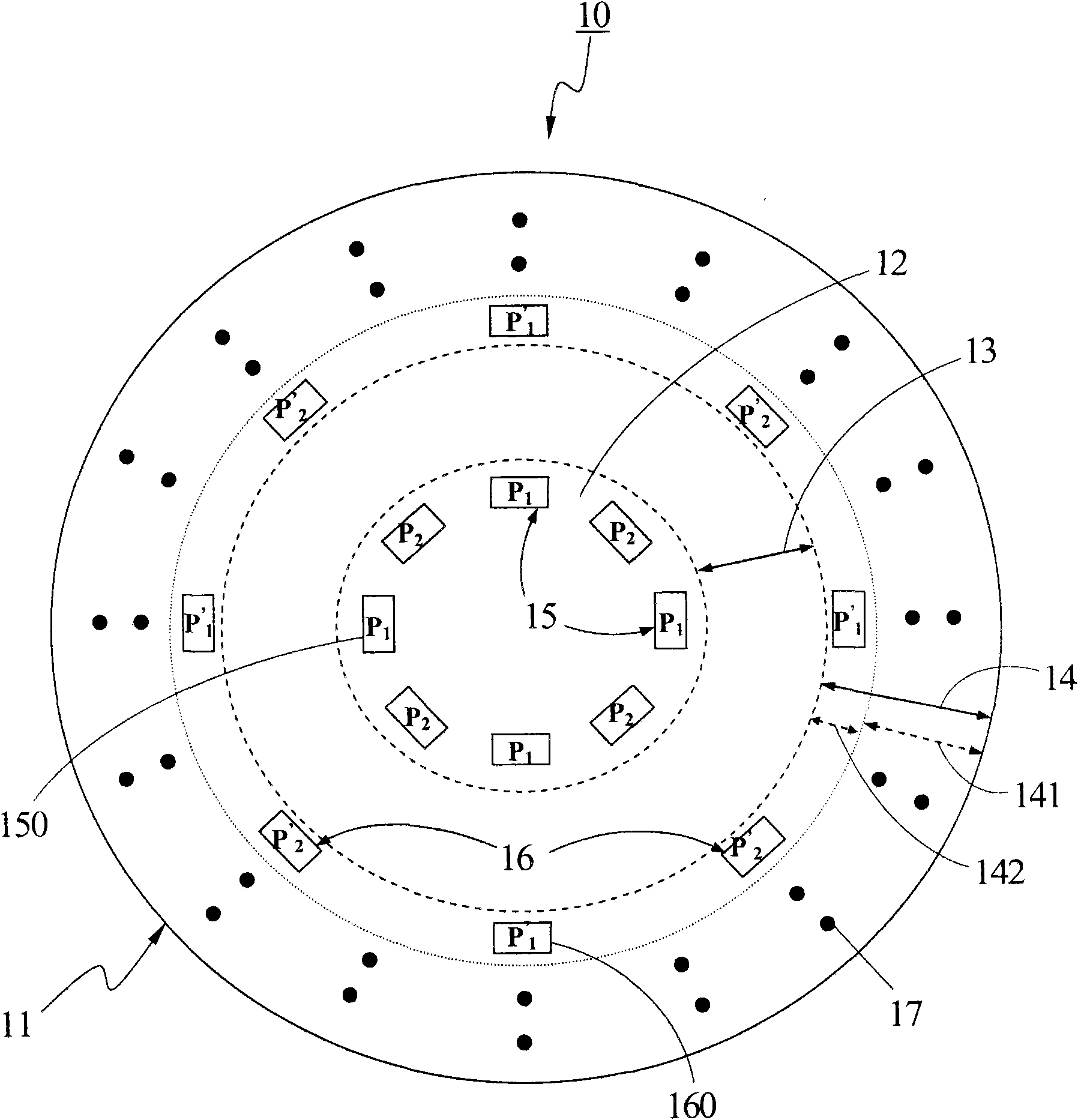
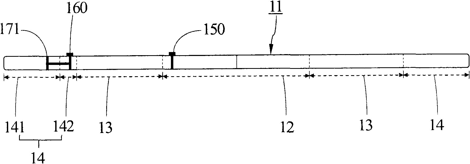
[0025] see Figure 2-1 and Figure 2-2 As shown, it is a schematic structural view and a schematic cross-sectional view of a printed circuit board 11 embodiment in the probe card 10 of the present invention. As shown in the figure: the printed circuit board 11 of this embodiment includes a solder joint area 12, a wiring area 13 and input area 14. Among them, the welding point area 12 is defined as the area where the printed circuit board 11 includes different pads and contacts for testing, power supply (power ring) near the inner ring; the input area 14 is defined as the printed circuit board 11 includes...


PUM


Abstract

The invention provides a probe card and a printed circuit board used for the same, which are used for promoting the power integrity during testing. The printed circuit board provided by the invention is defined as a welding spot area, a routing area and an input area, wherein the welding spot area comprises a plurality of first power welding pad groups; the input area comprises a plurality of second welding pad groups corresponding to the first power welding pad groups; and each first power welding pad group is insulated from each second welding pad group. The probe card provided by the invention adopts the printed circuit board and is combined with an external wire or an external power plane to obtain the better power integrity.

Description

technical field [0001] The invention relates to a probe card, in particular to a probe card with good power integrity; the invention also relates to a printed circuit board used for the probe card. Background technique [0002] When testing wafers or electronic components, the testing machine can use a probe card as a medium to input test signals from the probe card to a device under test (DUT), and pass through the probe The card returns the test results to the testing machine for subsequent detection and analysis. [0003] Taking wafer testing as an example, limited by factors such as the size and price of the testing machine, semiconductor factories usually can only use testing machines with a limited number and models to test the DUT. Since the test specifications, types, and quantities of the objects to be tested are different from each other, the testing machine cannot meet the test conditions of various processes or different types of objects to be tested when the te...

Claims


Application Information

Patent Timeline
IPC IPC(8): G01R1/067
Inventor 苏文彬谢昭平简志忠张庚生张嘉泰林书侃黄千惠张忠义何家齐
Owner MICROELECTRONICS TECH INC
Why Eureka
Try Eureka