Thin film transistor liquid crystal display (TFT-LCD) array substrate and manufacturing method thereof

A thin-film transistor and liquid crystal display technology, which is applied in semiconductor/solid-state device manufacturing, semiconductor devices, electric solid-state devices, etc., to achieve the effects of increasing area, facilitating implementation, and increasing aperture ratio

Active Publication Date: 2011-08-17
BOE TECH GRP CO LTD +1
View PDF4 Cites 21 Cited by
  • Summary
  • Abstract
  • Description
  • Claims
  • Application Information

AI Technical Summary

Problems solved by technology

Studies have shown that there is a light transmission phenomenon between the pixel electrode and the data line in this technical solution, which restricts the improvement of the aperture ratio to a certain extent. The liquid crystal is driven by the multi-dimensional space composite electric field, and the other part of the area is driven by the transverse electric field mode (In-Plane Switching, also known as in-plane switching).

Method used


Image

  • Thin film transistor liquid crystal display (TFT-LCD) array substrate and manufacturing method thereof
  • Thin film transistor liquid crystal display (TFT-LCD) array substrate and manufacturing method thereof
  • Thin film transistor liquid crystal display (TFT-LCD) array substrate and manufacturing method thereof

Examples


Embodiment Construction

[0060] The technical solutions of the present invention will be described in further detail below with reference to the accompanying drawings and embodiments. The film thicknesses and area sizes and shapes of the various layers in the drawings do not reflect the true proportions of the TFT-LCD array substrate, but are only intended to schematically illustrate the contents of the present invention.

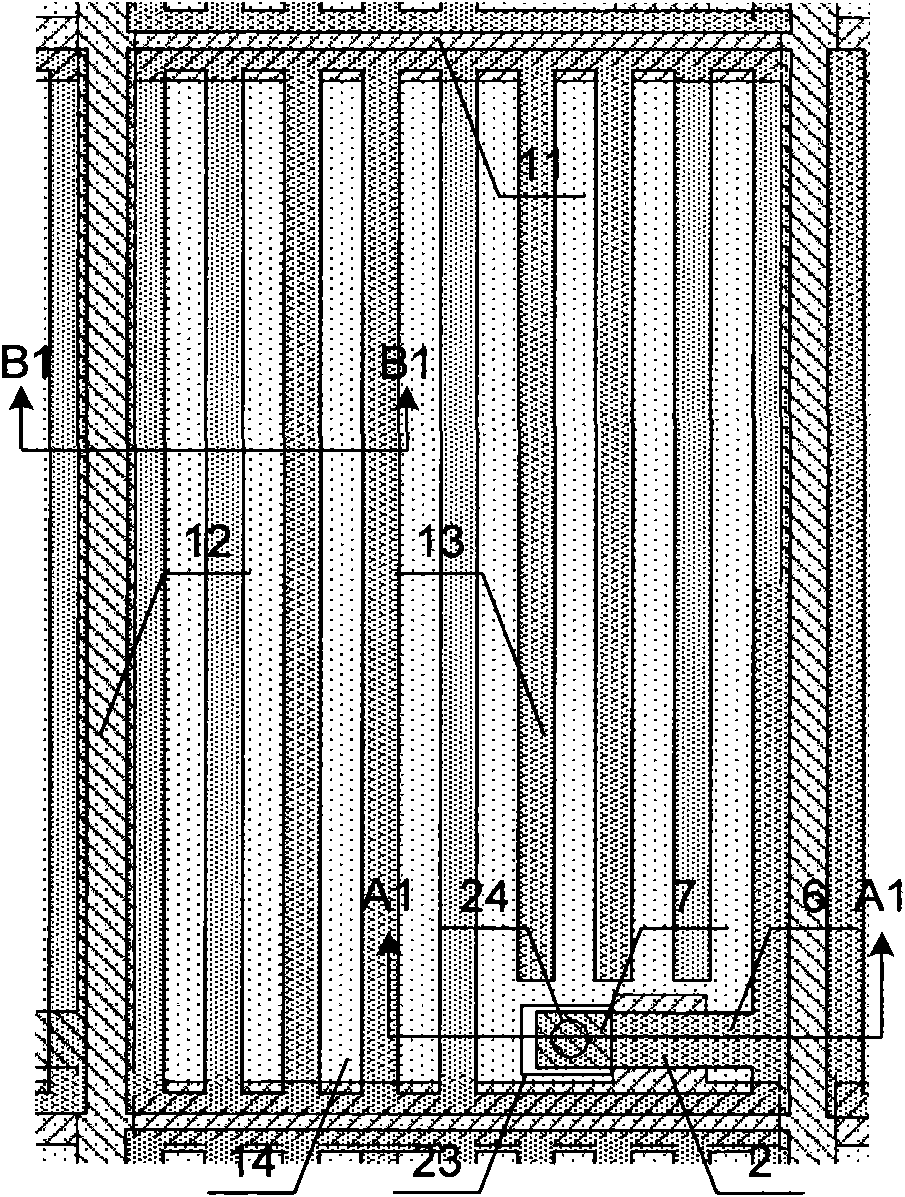
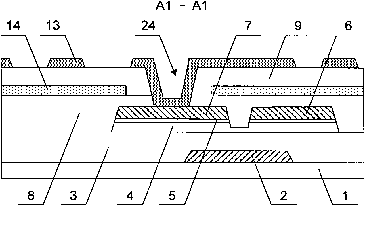
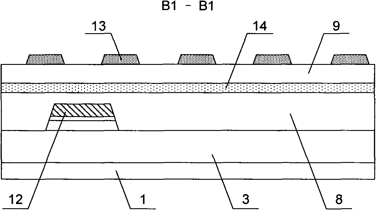
[0061] figure 1 It is a plan view of the TFT-LCD array substrate of the present invention, reflecting the structure of a pixel unit, figure 2 for figure 1 The cross-sectional view of A1-A1 in the middle, image 3 for figure 1 Sectional view of B1-B1 direction in the middle. Such as Figure 1 ~ Figure 3 As shown, the main structure of the TFT-LCD array substrate of the present invention includes gate lines 11, data lines 12, pixel electrodes 13, common electrodes 14 and thin film transistors formed on the substrate 1, and the gate lines 11 and data lines 12 define the pixel ar...


PUM


Abstract

The invention relates to a thin film transistor liquid crystal display (TFT-LCD) array substrate and a manufacturing method thereof. The array substrate comprises grid lines and data lines which define a pixel region, wherein a TFT, common electrodes and pixel electrodes of electrode strip structure are formed in the pixel region; the common electrodes are formed on a second insulating layer covering the data lines; and the pixel electrodes are formed on a third insulating layer covering the common electrodes. The array substrate and the manufacturing method have the following beneficial effects: by forming the common electrodes on the second insulating layer covering the data lines, forming the pixel electrodes of electrode strip structure on the third insulating layer covering the common electrodes and driving all the liquid crystals in the regions between the edges of the pixel electrodes and the edges of the data lines with a regular electric field, the efficiency of driving the liquid crystals is improved and the region becomes a display region, thus farthest increasing the area of the display region and effectively improving the aperture opening ratio.

Description

technical field [0001] The invention relates to a thin film transistor liquid crystal display and a manufacturing method thereof, in particular to a thin film transistor liquid crystal display array substrate and a manufacturing method thereof. Background technique [0002] In Thin Film Transistor Liquid Crystal Display (TFT-LCD) products, Advanced-Super Dimensional Switching (Advanced-Super Dimensional Switching; AD-SDS) is a technology that has emerged in recent years and can improve LCD picture quality. One of the most advanced technologies, it can achieve high penetration and large viewing angle requirements at the same time. AD-SDS technology forms a multi-dimensional space composite electric field through the parallel electric field generated by the edge of the pixel electrode in the same plane and the vertical electric field generated between the pixel electrode layer and the common electrode layer, so that the pixel electrodes in the liquid crystal cell, directly abo...

Claims


Application Information

Patent Timeline
Patent Type & Authority Applications(China)
IPC IPC(8): G02F1/1368G02F1/1343G02F1/1362H01L21/77H01L27/12
CPCG02F2201/40H01L27/124G02F1/134363G02F2001/134372G02F1/134372G02F1/1343G02F1/136
Inventor 金原奭金馝奭
Owner BOE TECH GRP CO LTD
Why Eureka
Try Eureka