

Method for determining illumination intensity distribution of light source and mask pattern of photo-etching process
A technology of light intensity and photolithography technology, which is applied in the field of integrated circuit manufacturing, can solve the problems of long calculation time and unsatisfactory effect, and achieve the effects of shortened calculation time, good effect and good optimization effect
- Summary
- Abstract
- Description
- Claims
- Application Information
AI Technical Summary
Problems solved by technology
Method used
Image

Examples
Embodiment Construction
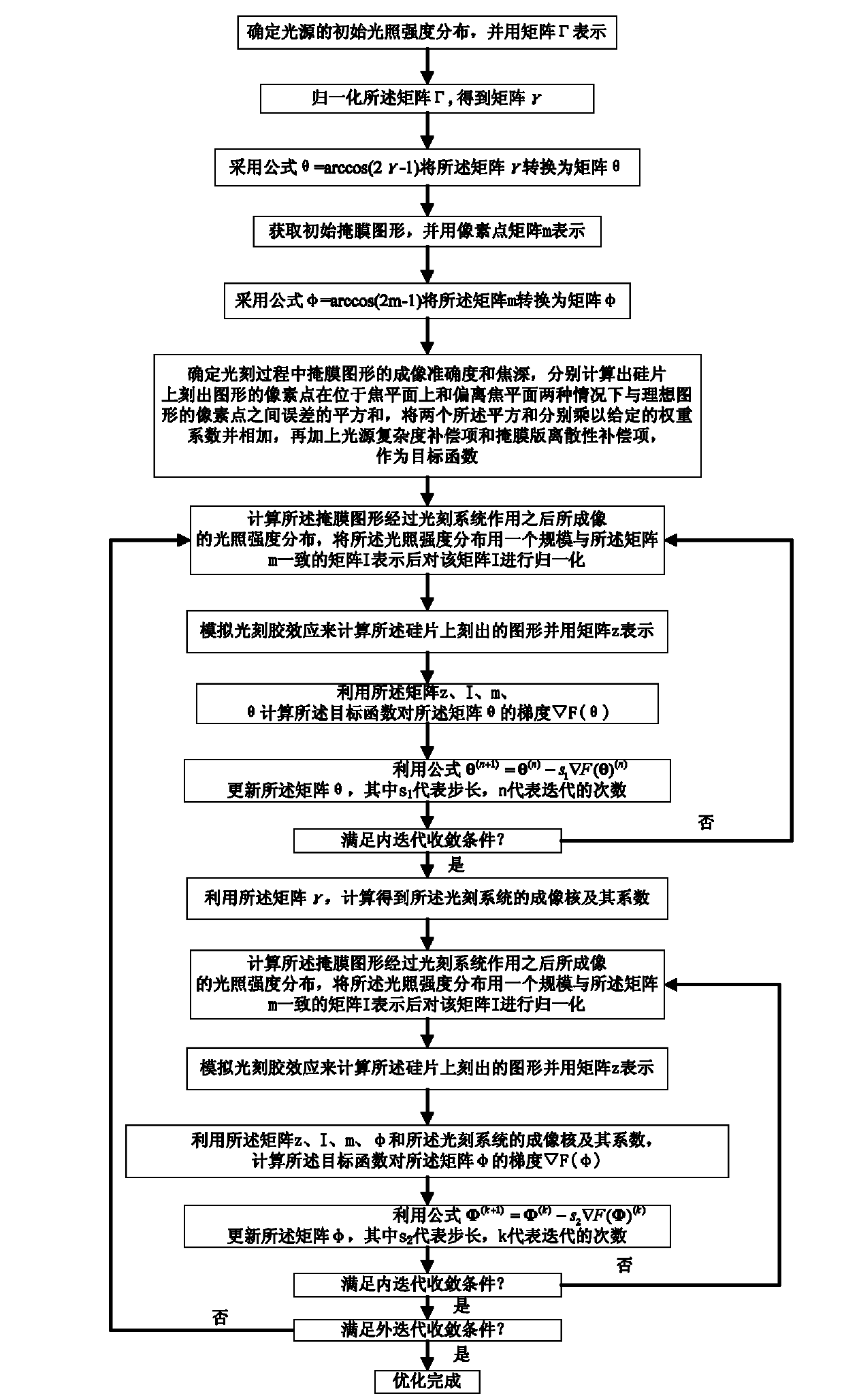
[0046] Embodiments of the present invention will be described in detail below in conjunction with the accompanying drawings.
[0047] figure 1 It is a flow chart of the method for optimizing the light source of the photolithography process according to the present invention. Such as figure 1 As shown, the method for determining the illumination intensity distribution of the photolithography process light source of the present invention comprises the following steps:
[0048] (1) Use matrix Γ to represent the initial illumination intensity distribution of the determined light source;
[0049] According to the traditional light sources used in the photolithography process in the current integrated circuit manufacturing, such as circular and ring-shaped light sources, determine the initial light intensity distribution of a light source, and use a matrix Γ to represent the light source, and each element in the matrix Γ is respectively Corresponding to a pixel at the correspondi...
PUM
 Abstract
Description
Claims
Application Information