Graphical substrate and light-emitting diode (LED) chip
A graphics substrate and graphics technology, applied in the direction of electrical components, circuits, semiconductor devices, etc., to achieve the effect of improving photoelectric performance, increasing luminous efficiency, and increasing the lateral epitaxy area
- Summary
- Abstract
- Description
- Claims
- Application Information
AI Technical Summary
Problems solved by technology
Method used
Image

Examples
Embodiment 1
[0079] Figure 3A It is a schematic diagram of a cross-sectional structure of a graphics substrate provided in Embodiment 1 of the present invention. Such as Figure 3A As shown, the graphics substrate includes a base substrate 10 and pattern bumps 101 arranged in an array form formed on the base substrate 10. The shape of the cross-section of the graphics bump 101 is trapezoidal, and the graphics bump mask 102 covers the graphics. The top surface of the protrusion 101. Figure 3B and Figure 3C It is a schematic structural diagram of the manufacturing process of the graphics substrate provided by Embodiment 1 of the present invention. Such as Figure 3B and Figure 3C As shown, the structure and formation process of each level in this embodiment may specifically be:
[0080] Such as Figure 3B Shown, at first, on the substrate 10 ', deposit one layer of thin film layer corresponding to pattern raised mask 102, then deposit a layer of photoresist, metal (Ni , Au, etc.)...
Embodiment 2
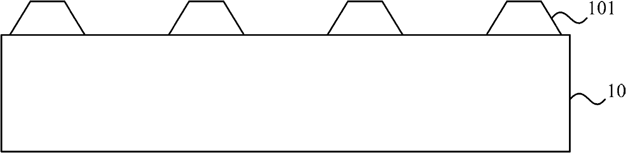
[0083] Figure 4A The schematic diagram of the cross-sectional structure of the graphics substrate provided in Embodiment 2 of the present invention, such as Figure 4A As shown, this includes the basic substrate 10 and the pattern protrusions 101 arranged in an array form on the basic substrate 10. The shape of the cross section of the pattern substrate pattern protrusions 101 is also trapezoidal, and the pattern substrate and the implementation The difference of the graphic substrate provided in Example 1 is that the graphic bump mask 102 covers the entire outer surface of the graphic bump 101 .
[0084] Figure 4B A schematic diagram of the threading dislocation structure during the epitaxy process on the patterned substrate provided by Embodiment 2 of the present invention, as shown in Figure 4BAs shown, the epitaxial layer 20 is grown on the patterned substrate in this embodiment, and there is no direct epitaxial growth on the patterned raised mask 102 because the patt...
Embodiment 3
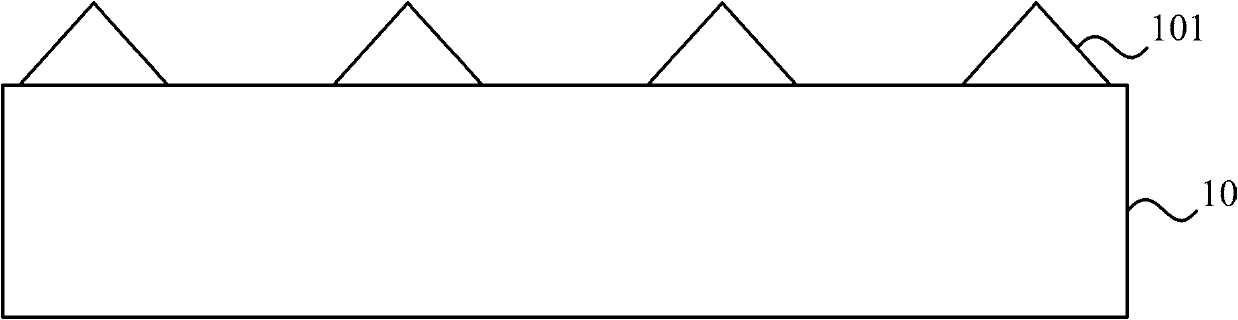
[0086] Figure 5A The schematic diagram of the cross-sectional structure of the graphics substrate provided in Embodiment 3 of the present invention, such as Figure 5A As shown, this includes a basic substrate 10 and patterned protrusions 101 arranged in an array formed on the basic substrate 10. The difference between the patterned substrate and the patterned substrate provided in Embodiment 2 is that the patterned substrate The shape of the cross section of the graphic protrusion 101 is triangular, and the graphic protrusion mask 102 covers the entire outer surface of the graphic protrusion 101 .
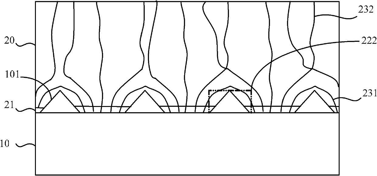
[0087] Figure 5B The schematic diagram of the threading dislocation structure during the epitaxy process on the patterned substrate provided by Embodiment 3 of the present invention, in the process of growing the epitaxial layer 20 on the patterned substrate in this embodiment, the dislocation loop 231 and threading dislocations formed Wrong 232 such as Figure 5B As shown, t...
PUM
 Abstract
Description
Claims
Application Information
 - R&D
- Intellectual Property
- Life Sciences
- Materials
- Tech Scout
- Unparalleled Data Quality
- Higher Quality Content
- 60% Fewer Hallucinations
Browse by: Latest US Patents, China's latest patents, Technical Efficacy Thesaurus, Application Domain, Technology Topic, Popular Technical Reports.
© 2025 PatSnap. All rights reserved.Legal|Privacy policy|Modern Slavery Act Transparency Statement|Sitemap|About US| Contact US: help@patsnap.com