Terahertz photon on chip control system and control method thereof

A technology of on-chip control and control methods, which is applied in the fields of optical waveguide light guide, semiconductor/solid-state device manufacturing, photometry using electric radiation detectors, etc., and can solve problems such as bulky far-field optical devices, large physical intervals, and low integration , to achieve the effect of wide application range, easy integration, novel and simple principle

Active Publication Date: 2011-09-07
SHANGHAI MUNICIPAL ELECTRIC POWER CO +1
View PDF3 Cites 4 Cited by
  • Summary
  • Abstract
  • Description
  • Claims
  • Application Information

AI Technical Summary

Problems solved by technology

Although the generation, propagation and detection of terahertz waves have developed rapidly in the past ten years, the current standard terahertz test systems are still assembled and configured by individual components, requiring the use of relatively large and bulky far-field optics. Devices, especially the terahertz source, detection, propagation and modulation parts are separated in various places in the system, the physical distance between them is relatively large, and the integration level is quite low

Method used


Image

  • Terahertz photon on chip control system and control method thereof
  • Terahertz photon on chip control system and control method thereof

Examples


Embodiment Construction

[0018] In order to make the object, technical solution and advantages of the present invention clearer, the present invention will be further described in detail below in conjunction with the accompanying drawings.

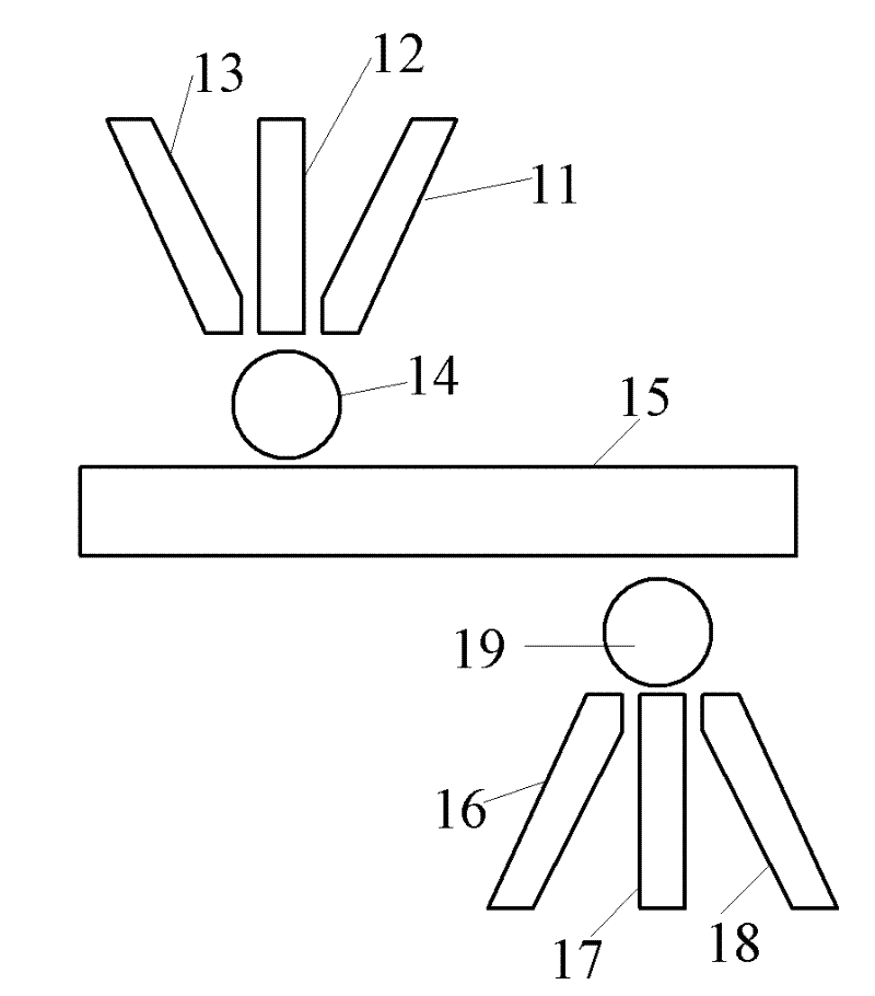
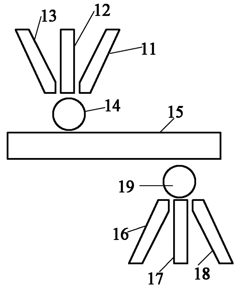
[0019] see figure 1 , figure 1 It is a structural schematic diagram of the terahertz photonic on-chip control system of the present invention. The terahertz photonic on-chip control system includes: a semiconductor heterojunction (not shown), a two-dimensional electron gas (not shown) formed on the surface of the semiconductor heterojunction, a Surface plasmon waveguide 15, terahertz source quantum dot formation structure, terahertz detection quantum dot formation structure. Preferably, the semiconductor heterojunction is GaAs semiconductor heterojunction or AlGaAs semiconductor heterojunction. The two-dimensional electron gas is about 1-100 nm away from the surface of the semiconductor heterojunction, and the electron mobility of the two-dimensional electron g...


PUM


Abstract

The invention relates to a terahertz photon on chip control system and a control method thereof. The system comprises a semiconductor heterojunction, a plasmon waveguide, a first source electrode, a first drain electrode, a first gate electrode, a second source electrode, a second drain electrode and a second gate electrode, wherein two-dimensional electron gases are formed on the surface of the semiconductor heterojunction; the first source electrode, the first drain electrode and the first gate electrode are formed on the surface of the semiconductor heterojunction and used for forming terahertz source quantum dots; and the second source electrode, the second drain electrode and the second gate electrode are formed on the surface of the semiconductor heterojunction and used for forming the terahertz source quantum dots. The terahertz photon on chip control system uses surface plasmon to integrate terahertz sources, detection, spread and modulation elements into a chip, thus realizing the terahertz photon on chip control.

Description

technical field [0001] The invention relates to a terahertz photonic on-chip control system and a control method thereof, in particular to a terahertz photonic on-chip control system and a control method thereof utilizing surface plasmons. Background technique [0002] Terahertz (THz, 1THz=10 12 Hz) band usually refers to the frequency range from 100 GHz to 10 THz, the corresponding wavelength is from 3 mm to 30 microns, and the electromagnetic spectrum range is quite wide between millimeter wave (submillimeter wave) and infrared light. However, for a long time, due to the lack of effective terahertz sources and detection methods, electromagnetic waves in the terahertz frequency band have not been fully studied and applied, which is called the "terahertz gap" in the electromagnetic spectrum. The advancement of terahertz technology has provided a great freedom for people to characterize and manipulate matter. It has been widely used in radio astronomy detection, atmospheric ...

Claims


Application Information

Patent Timeline
Patent Type & Authority Applications(China)
IPC IPC(8): H01L29/00H01L21/02G02B6/12G01J1/42
Inventor 钟旭
Owner SHANGHAI MUNICIPAL ELECTRIC POWER CO
Why Eureka
Try Eureka