Direct-current offset cancelling circuit applied to low-frequency variable gain amplifier

A technology of gain amplifier and DC offset, applied in the direction of amplification control, gain control, electrical components, etc., can solve the problems of affecting the compensation of DC offset accuracy, increasing area, increasing power consumption, etc., to reduce power consumption, eliminate DC offset, effect of reducing design complexity

Inactive Publication Date: 2011-09-07
BEIJING UNIV OF TECH
View PDF1 Cites 17 Cited by
  • Summary
  • Abstract
  • Description
  • Claims
  • Application Information

AI Technical Summary

Problems solved by technology

However, this method not only increases the area due to the introduction of an additional digital-to-analog converter, but also increases power consumption.
In addition, the non-ideal characteristics of the DAC and comparator itself can also affect the accuracy of compensating DC offset

Method used


Image

  • Direct-current offset cancelling circuit applied to low-frequency variable gain amplifier
  • Direct-current offset cancelling circuit applied to low-frequency variable gain amplifier
  • Direct-current offset cancelling circuit applied to low-frequency variable gain amplifier

Examples


Embodiment Construction

[0029] Specific embodiments of the present invention are described below in conjunction with the accompanying drawings:

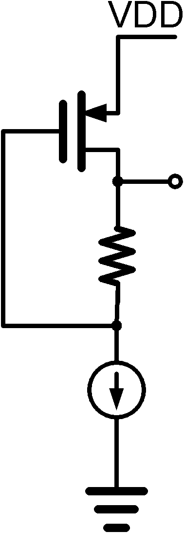
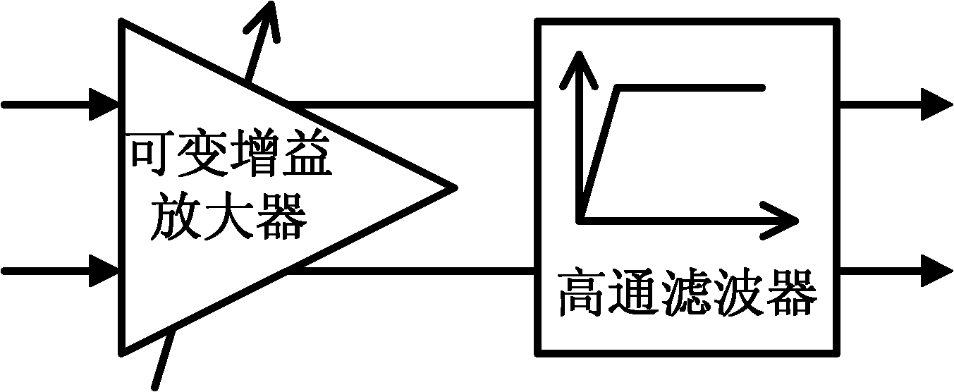
[0030] figure 1 A circuit diagram of a very small current source; figure 2 A circuit block diagram for the traditional high-pass filter to eliminate DC offset; image 3 A circuit block diagram for conventional DC offset removal using digital signal processing.

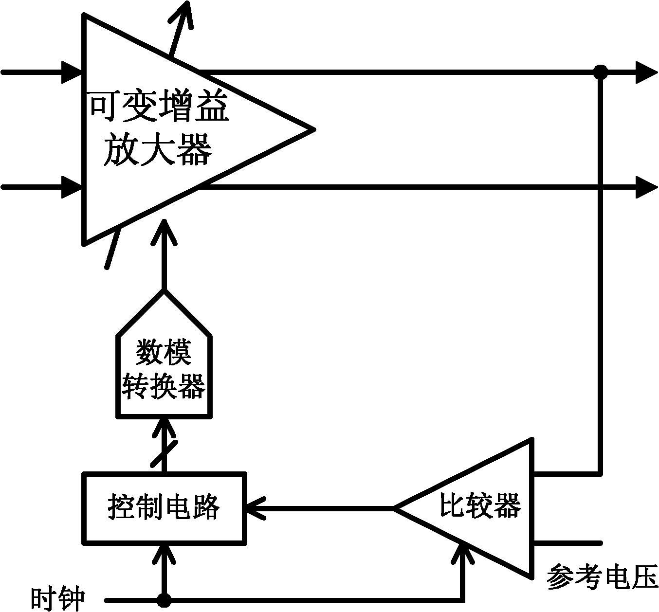
[0031] see Figure 4 As shown, the present invention is applied to the circuit block diagram of the embodiment of the low-frequency variable gain amplifier; including: a differential input pair, a current buffer, and a common-source output stage. Figure 4 The structure of variable gain amplifier using DC offset canceling circuit is given. The DC offset cancellation circuit consists of: a transconductance amplifier and a very small current source bias; the input of the transconductance amplifier is connected to the output of the variable gain amplifier for converting the output DC offset voltag...


PUM


Abstract

The invention discloses a direct-current offset cancelling circuit applied to a low-frequency variable gain amplifier, wherein the variable gain amplifier comprises an input differential pair, a current buffer and a common-source output stage; the direct-current offset cancelling circuit comprises a transconductance amplifier and a peaking current source for offsetting; the input of the transconductance amplifier is connected to the output end of the variable gain amplifier, and the transconductance amplifier is used for converting output direct-current offset voltage into current; and the output of the transconductance amplifier is connected to an output current additive node of a front-stage differential pair of the variable gain amplifier so as to constitute a negative feedback loop. The direct-current offset in a signal channel is corrected in real time by adopting the feedback loop of the transconductance amplifier and a peaking current source offset technology, rapid convergence can be realized in the process of initiating and switching gains, and the initial state of the variable gain amplifier is not limited. When the current additive node of the input signal channel accesses the feedback output of the transconductance amplifier, a peaking current source is used for offsetting the input stage of the transconductance amplifier.

Description

technical field [0001] The invention relates to a DC offset elimination circuit applied to a low-frequency variable gain amplifier, in particular to a method for eliminating the variable input of low-frequency signals by using a transconductance amplifier feedback circuit and a very small current source (peaking current source) bias. Gain Amplifier A circuit with a DC offset within the designed gain range. technical background [0002] The signal energy received from the antenna and optical cable is unpredictable, and the analog-to-digital converter has better linearity when the input swing is relatively large, so the communication system usually adds variable Gain amplifier, so that the input signal swing can be kept within a reasonable range, thereby improving the dynamic range of the system. [0003] Due to the evolution of the chip manufacturing process, the variable gain amplifier is limited in many aspects, and one of the non-ideal factors that cannot be ignored is th...

Claims


Application Information

Patent Timeline
Patent Type & Authority Applications(China)
IPC IPC(8): H03G3/30
Inventor 黄冠中吴颖杰钟超俐林平分
Owner BEIJING UNIV OF TECH
Why Eureka
Try Eureka