
Method for cleaning wafers between polishing stations

A polishing table and wafer technology, applied in grinding/polishing equipment, grinding/polishing safety devices, metal processing equipment, etc., can solve problems such as defects, wafer corrosion, and affecting wafer quality, and improve cleaning efficiency , Solve the effect of cleaning dead angle

Active Publication Date: 2016-03-09
SHANGHAI HUAHONG GRACE SEMICON MFG CORP
View PDF6 Cites 0 Cited by
  • Summary
  • Abstract
  • Description
  • Claims
  • Application Information

AI Technical Summary

Problems solved by technology

[0006] The problem to be solved by the present invention is that after an alarm is generated due to an abnormal situation during the polishing process of the wafer, the cleaning device between the polishing tables cannot effectively remove the polishing liquid on the wafer due to the existence of a cleaning dead angle, resulting in the corrosion of the surface of the wafer. defects that affect the quality of the wafer

Method used


Image

  • Method for cleaning wafers between polishing stations
  • Method for cleaning wafers between polishing stations
  • Method for cleaning wafers between polishing stations

Examples


Embodiment Construction

[0027] In order to make the above objects, features and advantages of the present invention more comprehensible, specific implementations of the present invention will be described in detail below in conjunction with the accompanying drawings.

[0028] In the following description, specific details are set forth in order to provide a thorough understanding of the present invention. However, the present invention can be implemented in many other ways than those described here, and those skilled in the art can make similar extensions without departing from the connotation of the present invention. Accordingly, the present invention is not limited to the specific embodiments disclosed below.

[0029] As mentioned in the background art, in the existing polishing process, when abnormalities occur in the working process of the CMP equipment, such as abnormalities in pressure and rotational speed, the CMP equipment will automatically stop working and issue an alarm. At this point, c...


PUM


Abstract

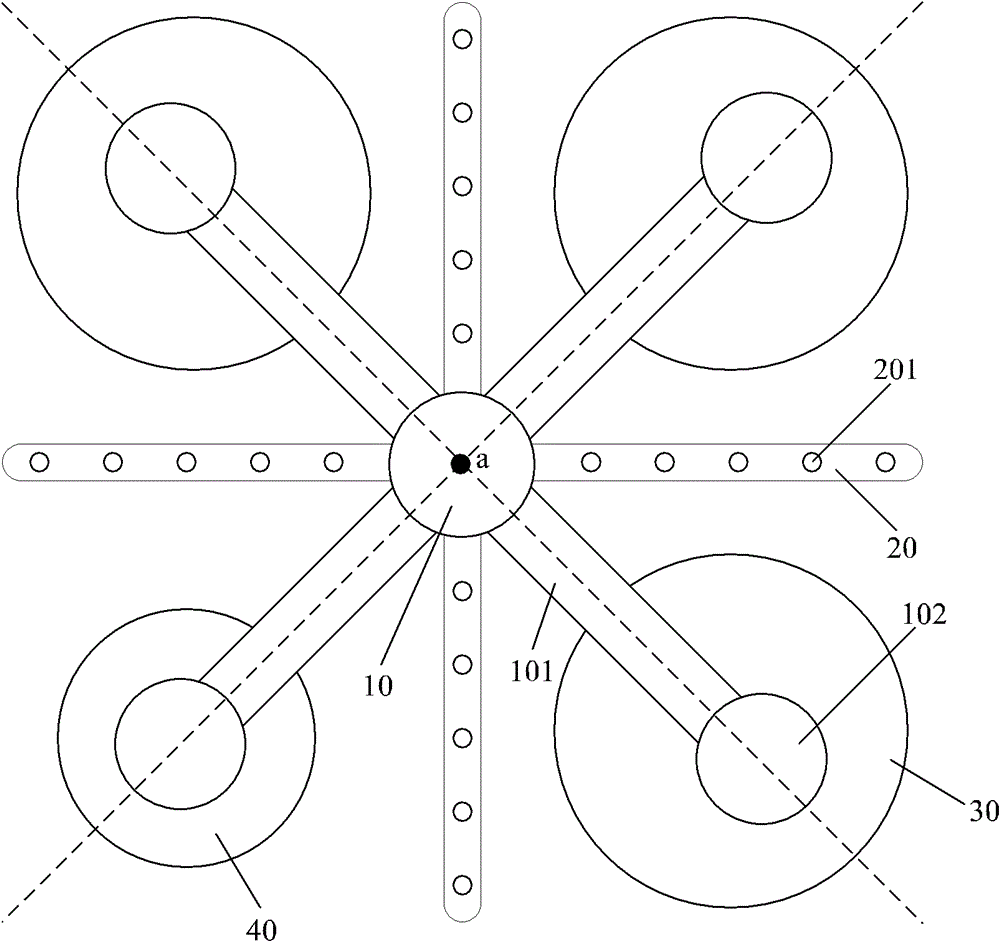
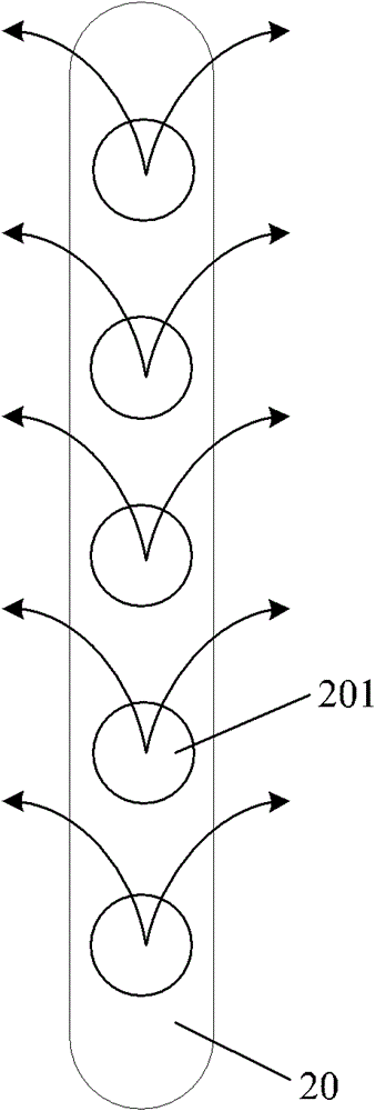
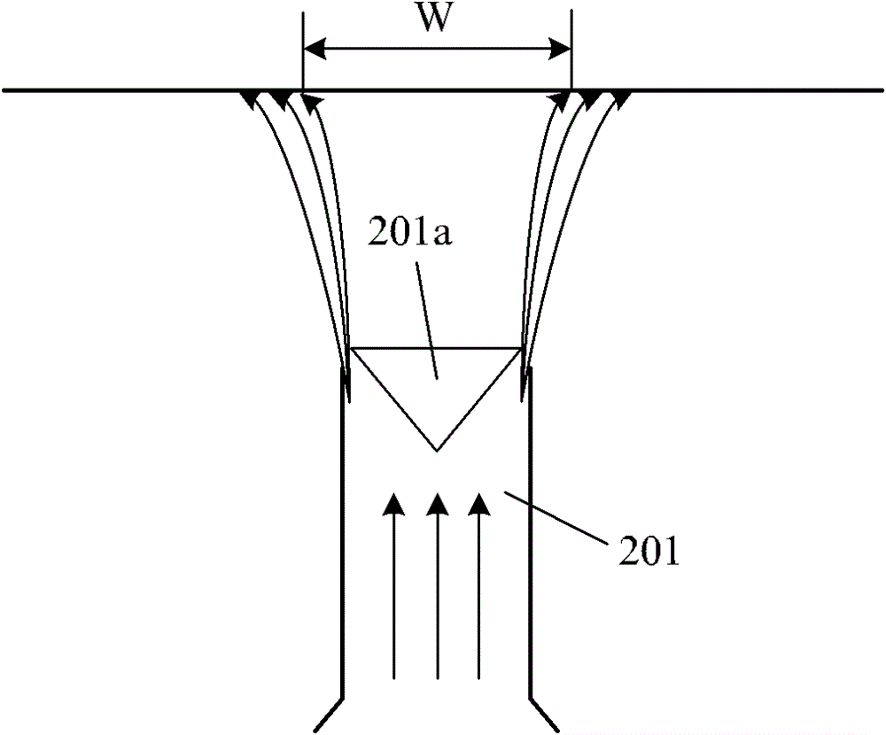
The invention relates to a method for cleaning wafers among polishing tables. The method comprises the following steps of: enabling a polishing head used for absorbing the wafers to deflect an angle Theta towards the position of 45 degrees among the polishing tables when a warning is given during polishing; enabling the wafer centers to deviate a distance D from a nozzle center line of a cleaning device among the polishing tables, wherein the D is not greater than half of the width of a cleaning dead angle formed by deionized water sprayed to the wafers by a nozzle; rotating the polishing head; and spraying the deionized water to the wafers. By the method, the problem of the cleaning dead angle formed during cleaning when the wafers rotate to the position of 45 degrees among the polishing tables, the defects caused by chemical corrosion of a polishing solution to the surfaces of the wafers are prevented, and the cleaning efficiency of the cleaning device among the polishing tables is also improved.

Description

technical field [0001] The invention relates to the field of semiconductor manufacturing, in particular to a method for cleaning wafers between polishing tables. Background technique [0002] The chemical mechanical polishing (CMP, ChemicalMechanicalPolishing) process was introduced into the integrated circuit manufacturing industry by IBM in 1984, and was first used in the planarization of the intermetal dielectric (IMD, InterMetalDielectric) in the subsequent process, and then used for Tungsten planarization, followed by shallow trench isolation (STI) and copper planarization. Chemical mechanical polishing is the fastest growing and most important technology in IC manufacturing process in recent years. The mechanism of CMP is that the surface material reacts chemically with the polishing material to form a relatively easy-to-remove surface layer, and the surface layer is mechanically worn away by the polishing agent in the polishing material and the relative movement of t...

Claims


Application Information

Patent Timeline
Patent Type & Authority Patents(China)
IPC IPC(8): B24B55/00
Inventor 李协吉李儒兴邵尔剑李志国
Owner SHANGHAI HUAHONG GRACE SEMICON MFG CORP
Learn More