Micro electromechanical device and manufacturing method thereof

A technology of a microelectromechanical device and a manufacturing method, which are applied in the directions of microstructure devices, processing microstructure devices, measuring devices, etc., can solve the problems of low integration, inability to meet portability, and large size of microelectromechanical devices, and meet the requirements of portability. performance, reduce volume, and improve integration

Active Publication Date: 2011-09-14
XIAN YISHEN OPTOELECTRONICS TECH CO LTD
View PDF3 Cites 18 Cited by
  • Summary
  • Abstract
  • Description
  • Claims
  • Application Information

AI Technical Summary

Problems solved by technology

Usually, the semiconductor substrate containing the control circuit and the semiconductor substrate on which the MEMS devices are formed are arranged side by side in the lead frame. T

Method used


Image

  • Micro electromechanical device and manufacturing method thereof
  • Micro electromechanical device and manufacturing method thereof
  • Micro electromechanical device and manufacturing method thereof

Examples


Embodiment Construction

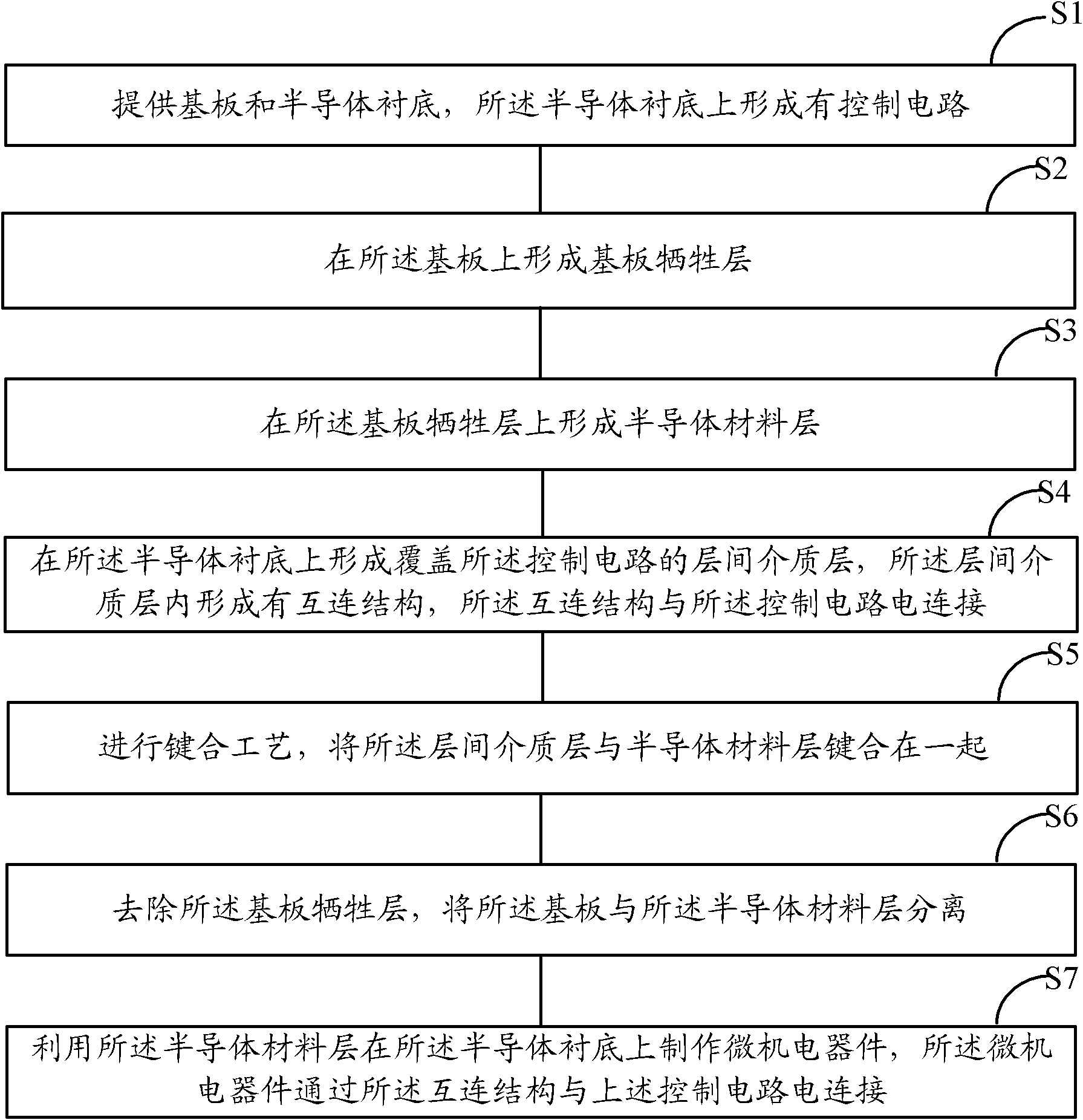
[0051] The micro-electro-mechanical device of the prior art is made by two semiconductor substrates, one of which is used to make a control circuit, and the other semiconductor substrate is used to make a micro-electro-mechanical device, and then the two semiconductor substrates are arranged side by side on the lead Therefore, the existing micro-electro-mechanical devices are large in size, so the integration degree of the micro-electro-mechanical devices is not high, and cannot meet the requirements of portability in applications. Moreover, in the prior art, two semiconductor substrates are used to fabricate one MEMS device, and the cost is relatively high.

[0052] Since the material of the movable electrode of the MEMS device is generally a semiconductor material layer, the semiconductor material layer may be a polysilicon layer, and the polysilicon layer is usually produced by a chemical vapor deposition process, and the temperature of the chemical vapor deposition process ...


PUM


Abstract

The invention provides a micro electromechanical device and a manufacturing method thereof. The manufacturing method comprises the following steps of: providing a base plate and a semiconductor substrate, wherein a control circuit is formed on the semiconductor substrate; forming a base plate sacrificial layer on the base plate; forming a semiconductor material layer on the base plate sacrificiallayer; forming an interlayer dielectric layer covering the control circuit on the semiconductor substrate, wherein an interconnection structure electrically connected with the control circuit is formed on the interlayer dielectric layer; performing a bonding process to bond the interlayer dielectric layer and the semiconductor material layer together; removing the base plate sacrificial layer, and separating the base plate and the semiconductor material layer; and manufacturing the micro electromechanical device electrically connected with the interconnection structure on the semiconductor substrate by using the semiconductor material layer. The embodiment of the invention improves the integration level of the micro electromechanical device to meet the requirement on portability in application.

Description

technical field [0001] Embodiments of the present invention relate to the technical field of semiconductors, in particular to micro-electromechanical devices and manufacturing methods thereof. Background technique [0002] MEMS (Micro Electro Mechanical System) technology refers to the technology of designing, processing, manufacturing, measuring and controlling micro / nano (micro / nanotechnology) materials. MEMS is a micro system that integrates mechanical components, optical systems, drive components, and electronic control systems into an integral unit. MEMS technology is generally applied in the manufacture of micro-electro-mechanical devices, which include: position sensors, rotation devices, or inertial sensors, such as acceleration sensors, gyroscopes, and sound sensors. [0003] The prior art utilizes MEMS technology to fabricate a micro-electromechanical device on a semiconductor substrate, then utilizes CMOS technology to fabricate a control circuit on another semic...

Claims


Application Information

Patent Timeline
IPC IPC(8): B81C3/00B81B7/00
Inventor 毛剑宏唐德明
Owner XIAN YISHEN OPTOELECTRONICS TECH CO LTD
Why Eureka
Try Eureka