Manufacturing method of nail head gold bump

A bump and stud head technology is applied in the field of stud head gold bump preparation, which can solve the problems of chip breakage, increase bonding force and bonding time, high material cost, etc., and achieve the effect of preventing failure and improving coplanarity.

Inactive Publication Date: 2011-09-14
SHANDONG UNIV OF TECH
View PDF6 Cites 8 Cited by
  • Summary
  • Abstract
  • Description
  • Claims
  • Application Information

AI Technical Summary

Problems solved by technology

However, the gold bump welding technology also has certain limitations: it is not suitable for high-density packaging; the material cost is very expensive; intermetallic compounds are easily generated between the gold bonding point and the aluminum metallization layer under high temperature conditions
If non-coplanarity is significant (for example, some bumps are taller than others), those lower bumps will not be able to contact the package substrate during flip-chip bonding, requiring significantly increased bond force and bond strength. time, so that all the bumps can be successfully bonded, but the fluctuation of bump height will lead to uneven distribution of bump loading force, chip breakage or open circuit, on the contrary, the improvement of bump coplanarity will reduce the impact on chip and substrate stress

Method used


Image

  • Manufacturing method of nail head gold bump
  • Manufacturing method of nail head gold bump
  • Manufacturing method of nail head gold bump

Examples


Embodiment Construction

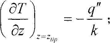
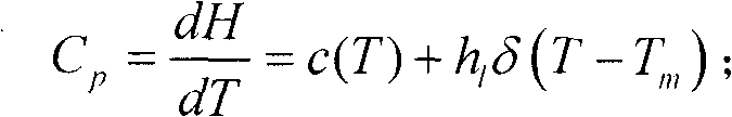
[0037] A method for preparing gold stud bumps with a gold ball size of 2 mils, comprising the following process: (1) through the image processing system, the rivet is accurately positioned above the pad, and the electronic discharge system is placed on the electronic spark rod A high voltage of 3kV is generated between the tail of the gold wire formed after the previous bonding cycle, and the formed arc generates high temperature to melt the bottom of the gold wire, and the first melted gold wire makes the liquid gold ball roll upwards under the action of surface tension Gold balls are formed, the discharge current is 30mA, and the discharge time is 0.8ms. The size of the gold balls depends on the energy when they are formed, and the energy depends on the temperature. The size of the gold balls determines the size of the gold bumps. Coplanarity, in order to improve the coplanarity of the gold bumps, the following equation is used to control the size of the gold balls:

[0038]...


PUM


Abstract

The invention relates to a manufacturing method of a nail head gold bump, comprising the following steps of: establishing an exact energy equation on the relation between a gold wire and a gold ball; vertically moving a riving knife upwards after a first welding point is finished, wherein an opened wire clip makes the gold wire slide in the riving knife and reach the expected height, i.e. the height of a welded gold bump; moving the riving knife at a certain speed rapidly rightwards, and keeping a slight connection between the gold wire and the gold ball; moving the riving knife upwards for a section of distance, and then closing the wire clip; continuously moving the riving knife upwards till the gold wire is pulled apart; and moving the riving knife to a place above a next bonding point to discharge and form a ball, and carrying out a next bonding circulation process. In the manufacturing method of the nail head gold bump disclosed by the invention, the sizes of formed balls are controlled, thus the coplanarity of the bump is improved, the bonding point is prevented from failure, and a high-speed high-precision manufacturing process of the gold bump is obtained.

Description

technical field [0001] The invention relates to a welding method in a microelectronic package, in particular to a method for preparing a nail head gold bump. Background technique [0002] At present, gold, copper, and aluminum are excellent materials for realizing chip-level interconnection technology in integrated circuit packaging. The most common and most successful metal lead used in gold bump bonding is gold wire. Gold has the advantages of high electrical conductivity, corrosion resistance, good toughness, etc., and the technology is mature and the process stability is good. However, the gold bump welding technology also has certain limitations: it is not suitable for high-density packaging; the material cost is very expensive; and intermetallic compounds are easily generated between the gold bonding point and the aluminum metallization layer under high temperature conditions. These intermetallic compounds have high contact resistance and high brittleness, and are pr...

Claims


Application Information

Patent Timeline
Patent Type & Authority Applications(China)
IPC IPC(8): H01L21/60
CPCH01L24/11H01L2224/11H01L2924/14H01L2924/00H01L2924/00012
Inventor 刘曰涛
Owner SHANDONG UNIV OF TECH
Why Eureka
Try Eureka