System and method for feeding back image quality of template for wafer alignment

A template image, quality feedback technology, applied in semiconductor/solid state device testing/measurement, electrical components, semiconductor/solid state device manufacturing, etc., can solve problems affecting image pattern pattern matching, manual intervention, pattern pattern matching failure, etc. Speed ​​up creation and increase success rate

Inactive Publication Date: 2011-09-14
上海高粱信息科技有限公司
View PDF5 Cites 23 Cited by
  • Summary
  • Abstract
  • Description
  • Claims
  • Application Information

AI Technical Summary

Problems solved by technology

For example, there are multiple layers of dielectric films on silicon (Si) wafers. They can be SiO2 and Si3N4. The interference between the interface and the interface with the silicon substrate will produce constructive or destructive light intensity, resulting in pattern changes in the image and affecting the pattern matching of the image mode
It is called color effect in the application, and it often causes pattern pattern matching to fail;
[0014] These problems may not be quantitatively known or foreseeable when the user creates a workflow for wafer alignment, but will only be encountered when the subsequent equipment automatically executes the workflow, resulting in image matching and even the entire wafer alignment failure
The consequences of wafer alignment failure in in-line equipment are severe and may require downtime for manual intervention, which means considerable losses for semiconductor integrated circuit manufacturers

Method used


Image

  • System and method for feeding back image quality of template for wafer alignment
  • System and method for feeding back image quality of template for wafer alignment
  • System and method for feeding back image quality of template for wafer alignment

Examples


Embodiment Construction

[0046] In order to make the technical means, creative features, goals and effects achieved by the present invention easy to understand, the present invention will be further described below in conjunction with specific illustrations.

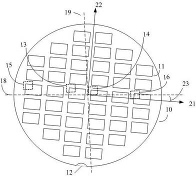
[0047] Such as figure 1 As shown, a template image quality feedback system for wafer alignment described in the present invention relates to semiconductor large-scale integrated circuit equipment, including a part of production and process inspection equipment, that is, it is used for wafer alignment Subsystem part. The present invention includes the subsystem and the method working on the system platform. During work, this method also can't avoid using certain specific semiconductor large-scale integrated circuit equipment where the subsystem of the present invention is located, such as the wafer pre-aligner on it, manipulator, mechanical motion platform, shared host computer and its software. , hardware, etc. Therefore, some components in th...


PUM


Abstract

The invention discloses a system and a method for feeding back the image quality of a template for wafer alignment. The system comprises a mechanical motion platform, a wafer tray, an industrial camera, an illumination device and a main computer, wherein the mechanical motion platform can freely move; and the wavelength range of illumination light waves of the illumination device can be changed. The software system comprises a user interface module, an image acquisition module, an image processing module and an equipment control module. A target image on the mechanical motion platform can be acquired in real time; after the target image is processed through a given algorithm in the software system; and normalized characteristics related to pattern recognition / template matching are extracted from the image and a template image and are displayed on a user interface in real time. The invention also discloses a method for finding the best matching template from given images.

Description

technical field [0001] The invention relates to the fields of image template recognition and image analysis, in particular to a system and method for feedbacking template image quality for wafer alignment on semiconductor large-scale integrated circuit manufacturing or process inspection equipment. Background technique [0002] In many semiconductor large-scale integrated circuit manufacturing or process testing equipment, all wafers involving integrated circuit patterns including logic units such as computer central processing units and storage units such as various computer memories are without exception due to extremely high precision requirements The first step is to perform wafer alignment. [0003] On-device wafer alignment is done in two parts. First of all, the operator creates the equipment workflow including where on the wafer and what kind of work to do to the wafer. For patterned wafers, the first step is how to do wafer alignment, because misaligned wafers Cir...

Claims


Application Information

Patent Timeline
Patent Type & Authority Applications(China)
IPC IPC(8): H01L21/66H01L21/68
Inventor 骊松·刘
Owner 上海高粱信息科技有限公司
Why Eureka
Try Eureka