Method for improving weak light response of amorphous silicon film battery

A technology of amorphous silicon thin film and battery, applied in the direction of circuits, electrical components, sustainable manufacturing/processing, etc., can solve the problems of interface defect density, stress concentration, etc., achieve weak light response improvement, eliminate heterojunction, and eliminate stress Effects of Concentration and Defect Density

Inactive Publication Date: 2011-09-14
HANGZHOU AMPLESUN SOLAR TECH
View PDF3 Cites 0 Cited by
  • Summary
  • Abstract
  • Description
  • Claims
  • Application Information

AI Technical Summary

Problems solved by technology

[0004] The technical problem to be solved and the technical task proposed by the present invention are to overcome the defects of stress concentration and interface defect density at the P / I interface caused by the heterojunction of the existing P-layer a-SiC and I-layer a-Si, and provide an improved Method for Weak Light Response of Amorphous Silicon Thin Film Cell

Method used


Image

  • Method for improving weak light response of amorphous silicon film battery
  • Method for improving weak light response of amorphous silicon film battery
  • Method for improving weak light response of amorphous silicon film battery

Examples


Embodiment 1

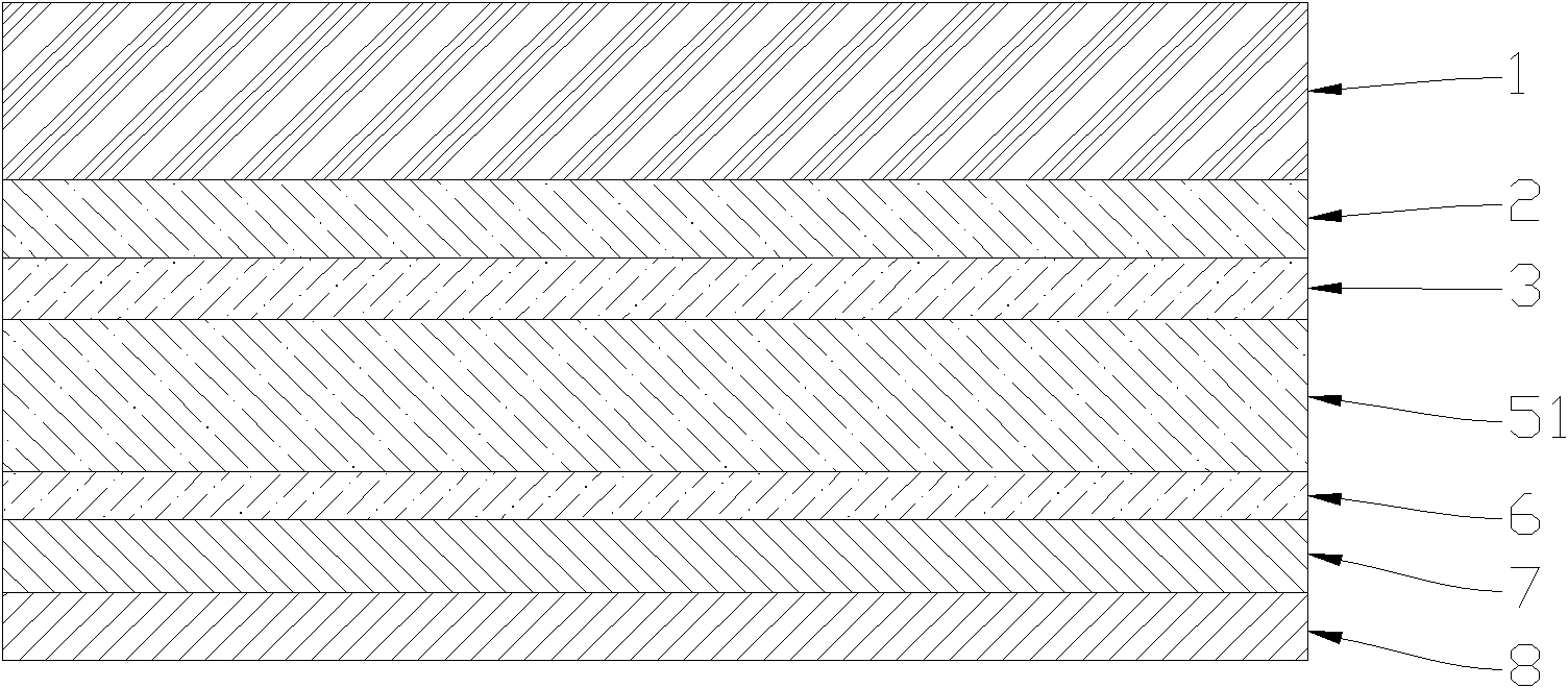
[0039] (1) Cleaning the transparent conductive oxide (TCO) substrate;

[0040] (2) On the TCO substrate, use plasma-enhanced chemical vapor deposition equipment to deposit an amorphous silicon film. Wherein the P layer deposition parameters are as follows:

[0041] Deposit the P-type layer on the transparent conductive glass, the deposition process parameters of the P layer are: SiH 4 、H 2 、CH 4 , TMB (trimethylboron or diethylalkane) gas, the deposition temperature is 180-260°C, and the deposition power density is 0.006-0.03W / cm 2 , the deposition pressure is 60-300Pa, CH 4 : SiH 4 The gas flow ratio is 40-70:100, and the deposition thickness is 10-20nm.

[0042] I layer through SiH 4 、H 2 、CH 4 gas, the deposition temperature is 180-260°C, H 2 : SiH 4 The dilution ratio is 2-20:1, and the deposition power density is 0.006-0.03W / cm 2 , the deposition pressure is 60-150Pa, CH 4 : SiH 4 The gas flow ratio is 7-10:100, and the deposition thickness is 150-500nm.

...

Embodiment 2

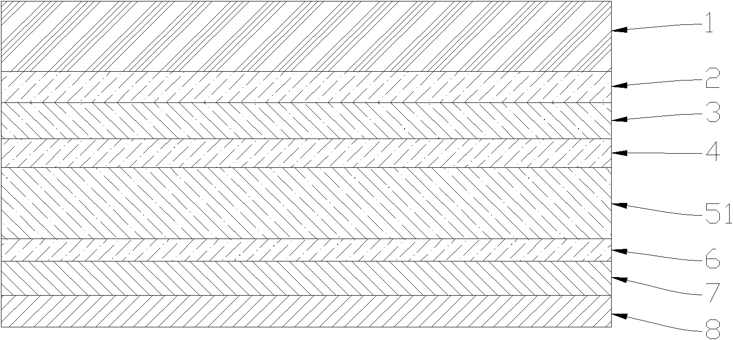
[0047] (1) Cleaning the transparent conductive oxide (TCO) substrate;

[0048] (2) On the TCO substrate, use plasma-enhanced chemical vapor deposition equipment to deposit an amorphous silicon film. Wherein the P layer deposition parameters are as follows:

[0049] Deposit the P-type layer on the transparent conductive glass, the deposition process parameters of the P layer are: SiH 4 、H 2 、CH 4 , TMB (trimethylboron or diethylalkane) gas, the deposition temperature is 180-260°C, and the deposition power density is 0.006-0.03W / cm 2 , the deposition pressure is 60-300Pa, CH 4 : SiH 4 The gas flow ratio is 40-70:100, and the deposition thickness is 10-20nm.

[0050] I layer through SiH 4 、H 2 、CH 4 gas, the deposition temperature is 180-260°C, H 2 : SiH 4 The dilution ratio is 2-20:1, and the deposition power density is 0.006-0.03W / cm 2 , the deposition pressure is 60-150Pa, CH 4 : SiH 4 The gas flow ratio is 13-20:100, and the deposition thickness is 150-500nm.

...

Embodiment 3

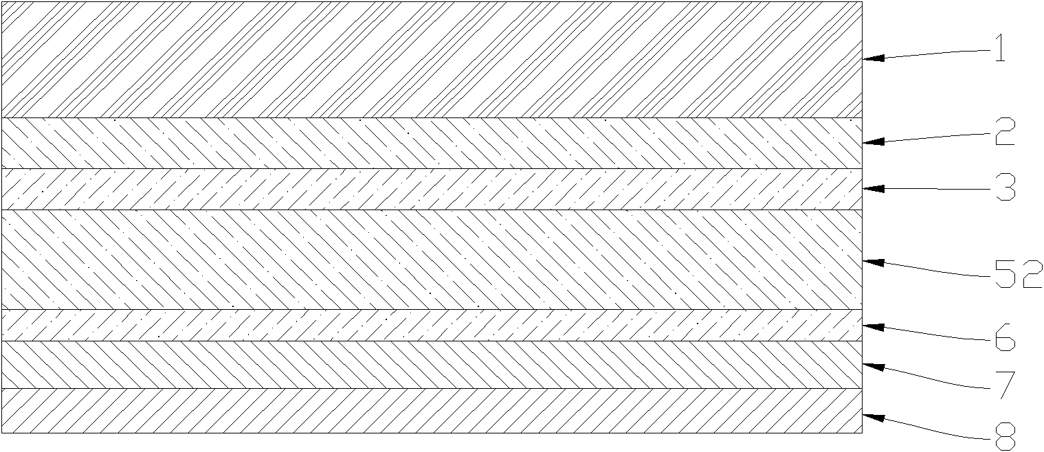
[0055] (1) Cleaning the transparent conductive oxide (TCO) substrate;

[0056] (2) On the TCO substrate, use plasma-enhanced chemical vapor deposition equipment to deposit an amorphous silicon film. Wherein the P layer deposition parameters are as follows:

[0057] Deposit the P-type layer on the transparent conductive glass, the deposition process parameters of the P layer are: SiH 4 、H 2 、CH 4 , TMB (trimethylboron or diethylalkane) gas, the deposition temperature is 180-260°C, and the deposition power density is 0.006-0.03W / cm 2 , the deposition pressure is 60-300Pa, CH 4 : SiH 4 The gas flow ratio is 40-70:100, and the deposition thickness is 10-20nm.

[0058] I layer through SiH 4 、H 2 、CH 4 gas, the deposition temperature is 180-260°C, H 2 : SiH 4 The dilution ratio is 2-20:1, and the deposition power density is 0.006-0.03W / cm 2 , the deposition pressure is 60-150Pa, CH 4 : SiH 4 The gas flow ratio is 23-33:100, and the deposition thickness is 150-500nm.

...


PUM


Abstract

The invention discloses a method for improving weak light response of an amorphous silicon film battery, belonging to the field of semiconductors. In the prior art, the heterojunction of a-SiC of a P layer and a-Si of an I layer causes stress concentration and defect density of a P / I interface. In the method, when raw materials containing gaseous H2 and gaseous SiH4 are used for depositing the P layer and the I layer on the basis of the decomposition reaction of the gaseous SiH4 to perform carbon element doping. The carbon element doping is to dope gaseous CH4 in the deposited raw materials. An a-Si layer of the I layer is converted into an a-SiC layer in a carbon doping mode, and the heterojunction of the a-SiC of the P layer and the a-Si of the I layer is further converted into a homojunction of the a-SiC of the P layer and the a-SiC of the I layer, thereby eliminating the heterojunction, and eliminating the stress concentration and defect density of the interface greatly, and finally improving the weak light response of the amorphous silicon film battery remarkably.

Description

technical field [0001] The invention relates to a method for improving the weak light response of an amorphous silicon thin film battery, in particular to a method for improving the weak light response of an amorphous silicon thin film battery by doping an intrinsic layer with carbon elements, and belongs to the field of semiconductors. Background technique [0002] Amorphous silicon thin-film batteries are developing rapidly because of their lower manufacturing cost than crystalline silicon bulk batteries, shorter energy recovery period, and more power generation at the same output power. At present, they are widely used in various outdoor power generation systems, such as photovoltaic power plants and curtain wall glass. , roof power generation system, etc. Relatively speaking, the current indoor application of amorphous silicon thin-film batteries is still relatively small, and there is a broad application potential, such as remote controls for various home appliances, th...

Claims


Application Information

Patent Timeline
IPC IPC(8): H01L31/20
CPCY02P70/50
Inventor 吴兴坤李媛曹松峰叶志高
Owner HANGZHOU AMPLESUN SOLAR TECH
Why Eureka
Try Eureka