Light-emitting diode and preparation method thereof, and solar cell and preparation method thereof

A technology of light emitting diodes and electrode layers, which is applied in the fields of photovoltaic power generation, circuits, electrical components, etc., can solve the problems of complex electrode preparation process of LED devices, and achieve the effect of improving compound efficiency.

Inactive Publication Date: 2011-09-14
SUZHOU NANOWIN SCI & TECH +1
View PDF6 Cites 13 Cited by
  • Summary
  • Abstract
  • Description
  • Claims
  • Application Information

AI Technical Summary

Problems solved by technology

[0005] The technical problem to be solved by the present invention is to provide a light-emitting diode and its preparation method, a solar cel

Method used


Image

  • Light-emitting diode and preparation method thereof, and solar cell and preparation method thereof
  • Light-emitting diode and preparation method thereof, and solar cell and preparation method thereof
  • Light-emitting diode and preparation method thereof, and solar cell and preparation method thereof

Examples


Embodiment Construction

[0020] The specific implementation of the light-emitting diode provided by the present invention and its preparation method will be described in detail below in conjunction with the accompanying drawings.

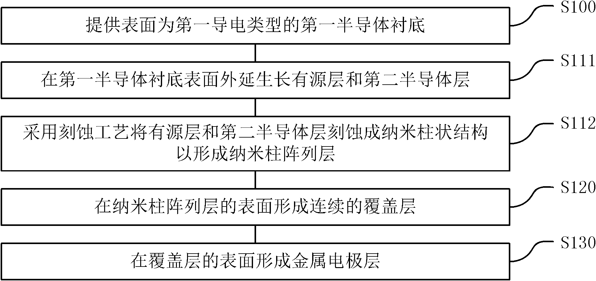
[0021] attached figure 1 Shown is a schematic diagram of the implementation steps of a specific embodiment of the present invention, including: Step S100, providing a first semiconductor substrate with a surface of the first conductivity type; Step S111, epitaxially growing an active layer and a second semiconductor substrate on the surface of the first semiconductor substrate. Semiconductor layer; step S112, using an etching process to etch the active layer and the second semiconductor layer into a nano-pillar structure to form a nano-pillar array layer; step S120, forming a continuous covering layer on the surface of the nano-pillar array layer; step S130, forming a metal electrode layer on the surface of the covering layer.

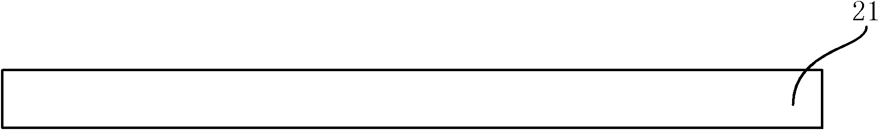
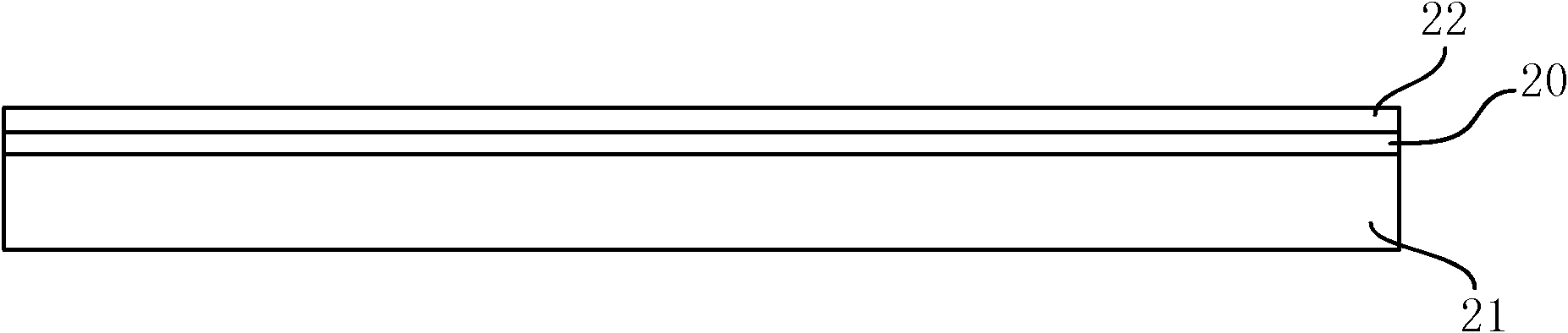
[0022] attached Figure 2A to attach Figu...


PUM


Abstract

The invention discloses a preparation method of a light-emitting diode. The method comprises the following steps of: providing a first semiconductor substrate having a first electric conduction type surface; forming a nanomcolumn array layer on the surface of the semiconductor substrate, wherein the nanomcolumn array layer comprises a second semiconductor layer having a second electric conduction type surface, and an active layer positioned below the second semiconductor layer and close to the first semiconductor substrate; forming a continuous graphene coating layer on the surface of the nanomcolumn array layer; and forming a metal electrode layer on the surface of the coating layer. The method has the advantages that: lattice mismatch of heterogenous junction material growth can be reduced; the composite efficiency of a charge carrier is improved; and the problems of low conversion efficiency and low stability of a multi-layer thin film and a horizontal structure caused by heating of a spreading resistor can be solved at the same time.

Description

technical field [0001] The invention relates to the technical field of semiconductor devices and processes, in particular to a light-emitting diode and a preparation method thereof, a solar cell and a preparation method thereof. Background technique [0002] At present, gallium nitride-based LEDs have become a new generation of green and environmentally friendly lighting sources due to their excellent characteristics such as good color selectivity, fast response speed, good stability, and high luminous efficiency. Huge application prospects. Gallium nitride-based LEDs are now mainly planar thin-film structures. Since the refractive index of gallium nitride-based semiconductors is generally significantly greater than that of air, a large part of the light generated inside the LED is reflected at the interface and will not contribute to effective luminescence. Nanopillars as optical waveguides provide the possibility to limit the propagation of light in a specific direction,...

Claims


Application Information

Patent Timeline
IPC IPC(8): H01L33/00H01L33/40H01L33/06H01L31/18H01L31/0224H01L31/0352H01L31/04H01L31/068
CPCY02E10/50Y02E10/547Y02P70/50
Inventor 樊英民王建峰刘争晖钟海舰任国强蔡德敏徐耿钊徐科
Owner SUZHOU NANOWIN SCI & TECH
Why Eureka
Try Eureka