Simple tristate input circuit

An input circuit and a simple technology, applied in the direction of logic circuit coupling/interface, logic circuit connection/interface layout using field effect transistors, etc., can solve the problems of increasing the number of IOs, increasing the cost of chip packaging, increasing chip power consumption, etc. , to achieve the effect of simple structure, excellent performance and reliable input signal

Active Publication Date: 2011-09-28
CHANGSHA JINGJIA MICROELECTRONICS
View PDF5 Cites 11 Cited by
  • Summary
  • Abstract
  • Description
  • Claims
  • Application Information

AI Technical Summary

Problems solved by technology

At the same time, the increase in the number of IOs will inevitably lead to an increase in chip power consumption and an increase in the cost of chip packaging.

Method used


Image

  • Simple tristate input circuit
  • Simple tristate input circuit
  • Simple tristate input circuit

Examples


Embodiment Construction

[0010] The present invention will be described in further detail below in conjunction with accompanying drawing and specific implementation:

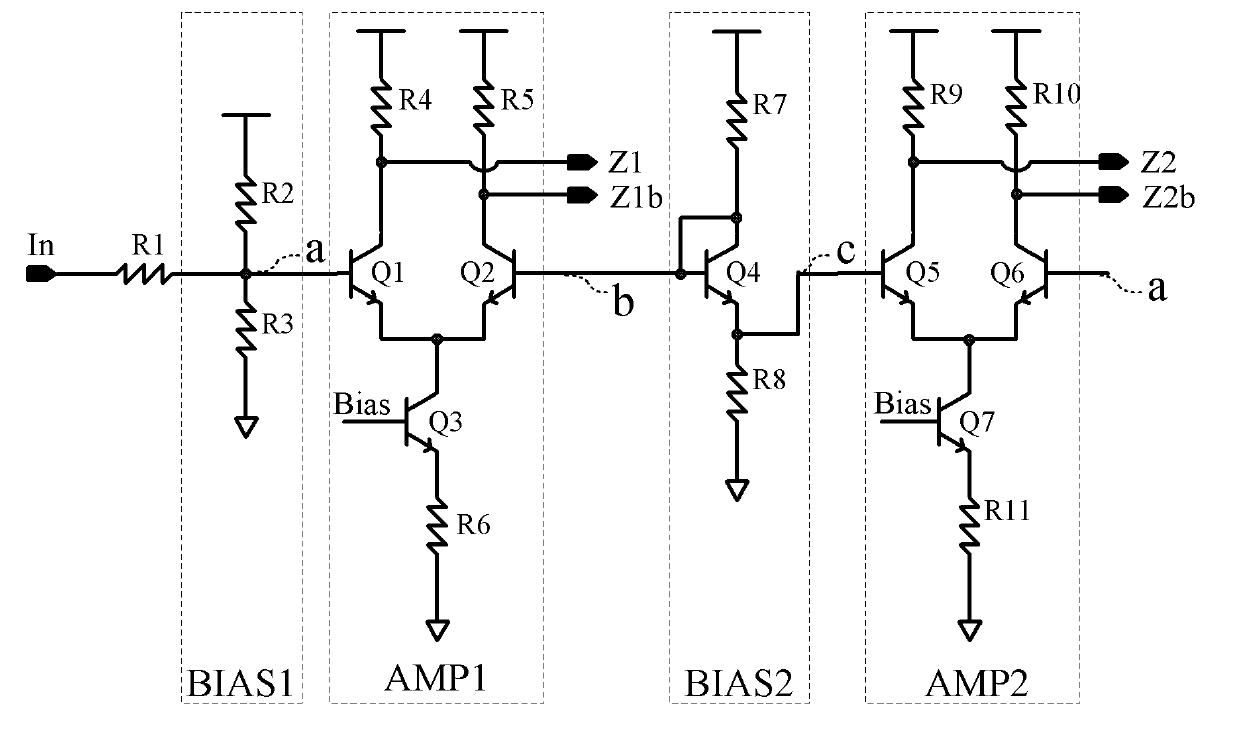
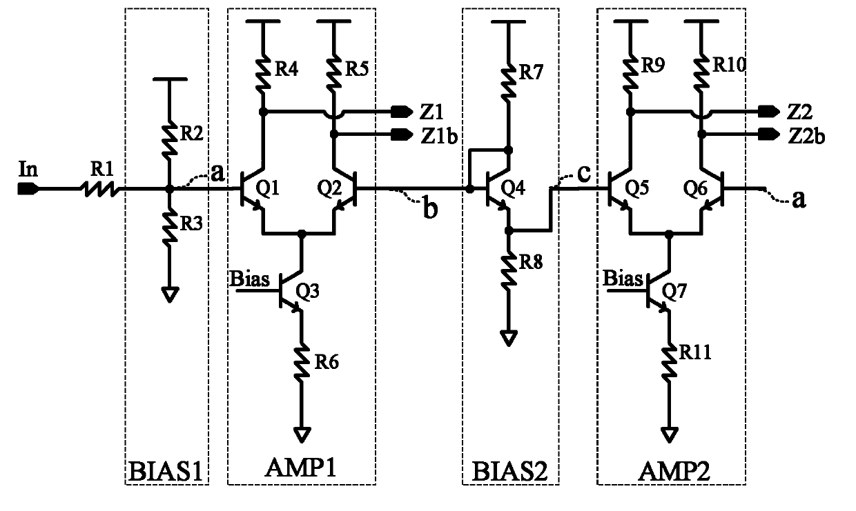
[0011] Such as figure 1 As shown, the circuit of the present invention is composed of four parts, bias circuits BIAS1, BIAS2, fully differential amplifiers AMP1, AMP2, and R1 is an input current limiting resistor. R2 and R3 are the same, and the resistance value is very large. Its function is to bias a to ,in is the power supply voltage; R7, triode Q4 and R8 form a bias circuit BIAS2, which biases the voltage of node b to , bias the voltage at node c to , that is, the voltage difference between node b and node c is The fully differential amplifier AMP1 composed of transistors Q1, Q2, Q3 and resistors R4, R5, R6, the inputs are a and b respectively, the outputs are Z1 and Z1b respectively, and the transistors Q5, Q6, Q7 and resistors R9, R10, R11 are composed of The fully differential amplifier AMP2 has inputs a and c, and outp...


PUM


Abstract

The invention discloses a tristate input circuit. In the circuit, the fact that bases and collectors of audions are in short circuit so as to have the characteristics of diodes is utilized, and one input end of two differential amplifiers is biased to two fixed voltages; the voltage D-value between the two fixed voltages is the conduction pressure drop Vbe of the diode; and the characteristic that the differential amplifiers are sensitive to a voltage difference is used to amplify the voltage D-value and output corresponding marking signals as well as detect that the input is in a high level, low level or suspension state, thus realizing the tristate input.

Description

technical field [0001] The invention mainly relates to the field of input IO circuit design, in particular to a three-state input circuit. Background technique [0002] Due to the advancement of manufacturing technology and the continuous improvement of design technology, more and more functional modules are integrated into the same chip, SOC is becoming more and more common, and the increase of functional modules will inevitably lead to an increase in input and output signals. , which will inevitably lead to an increase in the number of chip IOs. Because IO includes drivers and ESD logic, its area is usually large. For many control chips, due to the large number of IOs, its area is not limited by the area of ​​its own functional modules, but by the area of ​​​​the IO . At the same time, the increase in the number of IOs will inevitably lead to problems such as an increase in power consumption of the chip and an increase in the cost of chip packaging. [0003] In response...

Claims


Application Information

Patent Timeline
Patent Type & Authority Applications(China)
IPC IPC(8): H03K19/0185
Inventor 蒋仁杰陈怒兴郭斌
Owner CHANGSHA JINGJIA MICROELECTRONICS
Why Eureka
Try Eureka