Preparation method of silicon nano-wire field-effect transistor

A field-effect transistor, silicon nanowire technology, applied in nanotechnology, semiconductor/solid-state device manufacturing, electrical components, etc., can solve problems such as collapse, fracture of small silicon pillars, and difficulty in achieving uniform silicon pillars, and achieve optimal morphology, Process compatibility, the effect of shortening the molding time

Inactive Publication Date: 2011-10-12
XI AN JIAOTONG UNIV
View PDF5 Cites 25 Cited by
  • Summary
  • Abstract
  • Description
  • Claims
  • Application Information

AI Technical Summary

Problems solved by technology

The hollowing process is difficult to achieve uniform silicon pillars, and it is easy to cause small silicon pillars to break and collapse

Method used


Image

  • Preparation method of silicon nano-wire field-effect transistor
  • Preparation method of silicon nano-wire field-effect transistor
  • Preparation method of silicon nano-wire field-effect transistor

Examples


Embodiment Construction

[0057] The present invention is described in further detail below in conjunction with accompanying drawing:

[0058] In order to make the object, technical solution and advantages of the present invention clearer, the method for fabricating an n-type vertical silicon nanowire-enclosed gate field effect transistor will be further described in detail below in conjunction with specific embodiments and with reference to the accompanying drawings. The manufacturing method of the p-type vertical silicon nanowire-enclosed gate field effect transistor only needs to exchange the corresponding n-type and p-type regions in the process.

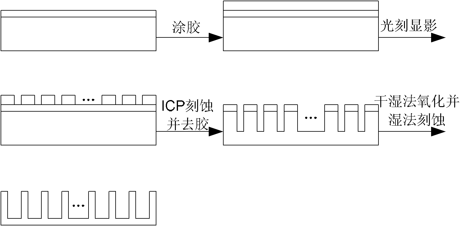
[0059] Step 1: Follow the figure 1 Shown is the flow chart of the process for fabricating vertical silicon nanowires.

[0060] First: SiO growth on cleaned substrate 2 Dielectric layer, gluing, pre-baking, exposure, development, film hardening.

[0061] The substrate is a P-type (100) silicon substrate, and the silicon chip is passed through acetone, ...


PUM


Abstract

The invention relates to the field of microelectronic apparatus manufacture, and discloses a top-down preparation method of a vertical silicon nano-wire gate field-effect transistor. The vertical silicon nano-wire gate field-effect transistor includes a semiconductor substrate, a nano-wire channel region vertically arranged on the semiconductor substrate and an annular grid conductive layer arranged out of the channel. The nano-wire channel region is provided with an active conductive layer; the upper part is doped with n impurity to serve as a source end n area; the semiconductor substrate contacting with the bottom of the drain conductive layer is doped with n impurity to serve as a drain end n area; and a non-symmetrical Halo-doped structure p+ region is added between the source end and the channel. The method for preparing the vertical silicon nano-wire gate field-effect transistor can well control the consistency of the position and size of the nano-wire, thus simplifying the manufacture process and reducing the manufacture cost.

Description

Technical field: [0001] The invention relates to the field of manufacturing nanometer electronic devices, in particular to a method for preparing a field-effect transistor surrounded by vertical silicon nanowires. Background technique: [0002] The increase in integrated circuit density, the continuous improvement in performance, and the continuous decline in cost benefit from the continuous reduction in the size of MOS devices. However, when the size of MOS devices is reduced to the nanometer level, the short channel and subthreshold performance degrade rapidly. In order to suppress the performance degradation of MOS devices and enable integrated circuits to still have good performance at the nanometer level, innovations can be made in terms of device structure. Change the traditional planar device structure to a multi-gate MOS structure to increase the control ability of the gate to the channel. Because the entire channel is surrounded by the gate, the surrounding gate d...

Claims


Application Information

Patent Timeline
Patent Type & Authority Applications(China)
IPC IPC(8): H01L21/336B82Y40/00
Inventor 李尊朝尤一龙李昕怡黎相孟崔吾元
Owner XI AN JIAOTONG UNIV
Why Eureka
Try Eureka