Combined type high-power semiconductor chip

A high-power, semiconductor technology, used in semiconductor devices, semiconductor/solid-state device components, electric solid-state devices, etc., can solve the problem of high cost, achieve the effect of eliminating thermal stress, high efficiency, and reducing production costs

A high-power, semiconductor technology, used in semiconductor devices, semiconductor/solid-state device components, electric solid-state devices, etc., can solve the problem of high cost, achieve the effect of eliminating thermal stress, high efficiency, and reducing production costs

CN102214642BActive Publication Date: 2012-10-10ANHUI PROVINCE QIMEN COUNTY HUANGSHAN ELECTRIC APPLIANCE

Image

  • Combined type high-power semiconductor chip
  • Combined type high-power semiconductor chip

Examples


Embodiment Construction

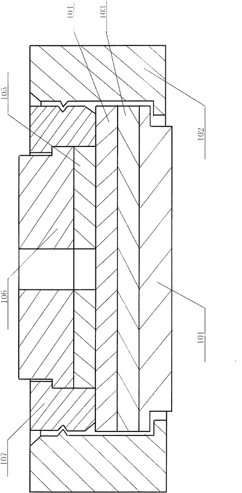
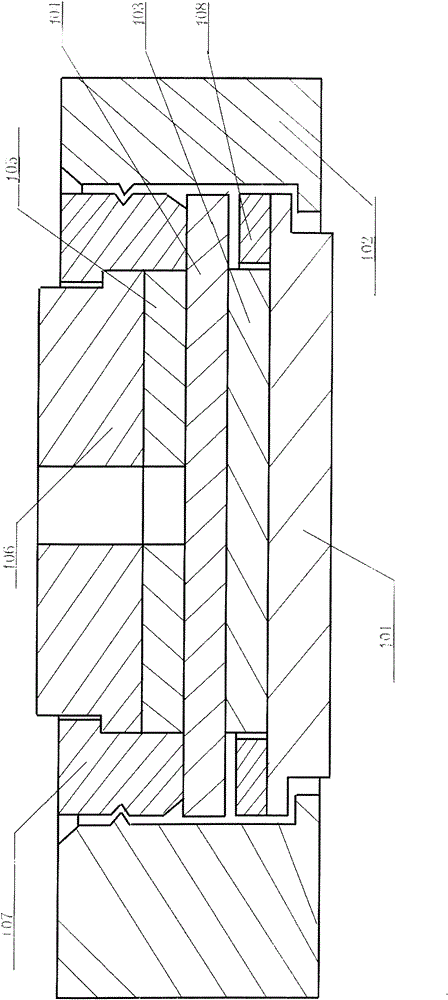
[0011] Such as figure 1 As shown, a combined high-power semiconductor chip includes a package body, a chip, a molybdenum sheet and a copper sheet. The package body is an inner and outer special-shaped annular ring. The upper inner wall of the outer special-shaped annular ring 102 is provided with an inwardly convex snap ring, and the bottom is provided with at least two inwardly convex stoppers. The upper plane of the outer special-shaped annular ring intersects the inner wall. There are chamfers. The outer edge of the inner special-shaped annular ring 107 is provided with a groove that matches the snap ring on the inner wall of the outer special-shaped annular ring, and its upper end is at least provided with two or more inwardly convex stoppers. Chamfers are provided where the planes meet. The inner and outer special-shaped annular rings are made of PPS insulating plastic. A lower copper sheet 101 , a lower molybdenum sheet 103 , a chip 104 and an inner shaped annular rin...


PUM


Abstract

The invention provides a combined type high-power semiconductor chip and belongs to the technical field of power electronic semiconductor devices. The combined type high-power semiconductor chip comprises a package body, a chip, molybdenum pieces and copper pieces, wherein the package body comprises an inner abnormally-shaped annular ring and an outer abnormally-shaped annular ring; an inward protruded clamping ring is arranged on the inner wall of the upper part of the outer abnormally-shaped annular ring (102); an inward protruded limiting block is arranged at the bottom of the outer abnormally-shaped annular ring (102); a groove which is combined with the clamping ring on the inner wall of the outer abnormally-shaped annular ring in a matched way is arranged on the outer edge of the inner abnormally-shaped annular ring (107); an inward protruded limiting block is arranged at the upper end of the inner abnormally-shaped annular ring (107); a lower copper piece (101), a lower molybdenum piece (103), the chip (104) and the inner abnormally-shaped annular ring are arranged in the outer abnormally-shaped annular ring; and an upper molybdenum piece (105) and an upper copper piece (106) are arranged in the inner abnormally-shaped annular ring. By the combined type high-power semiconductor chip, the chip, the molybdenum pieces and the copper pieces can be compressed with one another according to pressure of an outer clamping device, and aims of high product yield, low thermal stress, improvement on thermal cycle frequency, low cost, and convenience and quickness of assembly arefulfilled.

Description

Technical field: [0001] The invention relates to a combined high-power semiconductor chip, which belongs to the technical field of power electronic semiconductor chips. Background technique: [0002] Power electronic semiconductor chips refer to semiconductor devices such as rectifier diodes, fast rectifier diodes, thyristors and fast thyristors in the field of power electronic devices. Most of the low-power chip anode and cathode are welded together with soft solder and molybdenum sheet to form a die. The chips with high power above 200A are welded together by molybdenum and silicon chips. Generally, the molybdenum sheet is welded on the anode side of the semiconductor chip. Welding directly places the chip between two molybdenum sheets, and relies on the pressure of the external clamping device to press the chip and the molybdenum sheet together. [0003] However, both of the above methods have disadvantages: [0004] The welding type has a large thermal stress, and the...

Claims


Application Information

Patent Timeline
10 Oct 2012
Publication
CN102214642B
IPC
H01L25/00; H01L23/31
Inventors
王日新; 王民安