White light organic electroluminescent device and manufacturing method thereof
An electroluminescent device, an organic technology, applied in the direction of electric solid-state devices, chemical instruments and methods, semiconductor/solid-state device manufacturing, etc., to achieve the effects of improving efficiency, broadening the exciton recombination area, and eliminating non-radiative recombination energy loss
- Summary
- Abstract
- Description
- Claims
- Application Information
AI Technical Summary
Problems solved by technology
Method used
Image

Examples
Embodiment 1
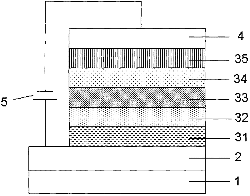
[0058] Such as figure 2 As shown, the material of the hole transport and exciton blocking layer 31 of the device is TAPC, the blue phosphorescent light emitting layer 32 selects the blue phosphorescent material Firpic doped with mCP, the spacer layer 33 selects the wide bandgap hole transport type material mCP, and the complementary phosphorescence The light-emitting layer 34 selects yellow phosphorescent dye (t-bt) 2 Ir(acac) doped BPhen, the electron transport layer 35 is made of BPhen, and the cathode layer 4 is made of Mg:Ag alloy and Ag. The entire device structure is described as:
[0059] Glass / ITO / TAPC(30nm) / mCP:Firpic(20nm) / mCP(5nm) / BPhen:(t-bt) 2 Ir(acac)(15nm) / BPhen(40nm) / Mg:Ag(200nm) / Ag(10nm)
[0060] The preparation method is as follows:
[0061] ①Use detergent, deionized water, acetone solution and ethanol solution to ultrasonically clean the glass substrate and the transparent conductive film ITO on it, and dry it with high-purity nitrogen after cleaning. ...
Embodiment 2
[0068] Such as figure 2 As shown, the material of the hole transport and exciton blocking layer 31 of the device is TAPC, the blue phosphorescent light emitting layer 32 selects the blue phosphorescent material Firpic doped with mCP, the spacer layer 33 selects the wide bandgap hole transport type material mCP, and the complementary phosphorescence The light-emitting layer 34 selects green phosphorescent dye (tpbi) 2 Ir(acac) doped BPhen, the electron transport layer 35 is made of BPhen, and the cathode layer 4 is made of Mg:Ag alloy and Ag. The entire device structure is described as:
[0069] Glass / ITO / TAPC(30nm) / mCP:Firpic(20nm) / mCP(5nm) / BPhen:(tpbi) 2 Ir(acac)(15nm) / BPhen(40nm) / Mg:Ag(200nm) / Ag(10nm)
[0070] The fabrication process of the device is similar to that of Example 1.
Embodiment 3
[0072] Such as figure 2 As shown, the material of the hole transport and exciton blocking layer 31 of the device is TAPC, the blue phosphorescent light-emitting layer 32 selects the blue phosphorescent material FIr6 doped with mCP, the spacer layer 33 selects the wide bandgap hole transport type material mCP, and the complementary phosphorescence The light-emitting layer 34 selects yellow phosphorescent dye (t-bt) 2 Ir(acac) doped BPhen, the electron transport layer 35 is made of BPhen, and the cathode layer 4 is made of Mg:Ag alloy and Ag. The entire device structure is described as:
[0073] Glass / ITO / TAPC(30nm) / mCP:FIr6(20nm) / mCP(5nm) / BPhen:(t-bt) 2 Ir(acac)(15nm) / BPhen(40nm) / Mg:Ag(200nm) / Ag(10nm)
[0074] The fabrication process of the device is similar to that of Example 1.
PUM
| Property | Measurement | Unit |
|---|---|---|
| Sheet resistance | aaaaa | aaaaa |
| Film thickness | aaaaa | aaaaa |
Abstract
Description
Claims
Application Information
 - R&D
- Intellectual Property
- Life Sciences
- Materials
- Tech Scout
- Unparalleled Data Quality
- Higher Quality Content
- 60% Fewer Hallucinations
Browse by: Latest US Patents, China's latest patents, Technical Efficacy Thesaurus, Application Domain, Technology Topic, Popular Technical Reports.
© 2025 PatSnap. All rights reserved.Legal|Privacy policy|Modern Slavery Act Transparency Statement|Sitemap|About US| Contact US: help@patsnap.com