Method for fabricating a gate dielectric layer

A gate dielectric layer and manufacturing method technology, applied in semiconductor/solid-state device manufacturing, circuits, electrical components, etc., can solve the problems of reduction, increase of equivalent thickness of high dielectric constant gate dielectric layer 112, etc., to achieve The effect of maintaining the performance characteristics of the device

Active Publication Date: 2011-10-19
TAIWAN SEMICON MFG CO LTD
View PDF4 Cites 0 Cited by
  • Summary
  • Abstract
  • Description
  • Claims
  • Application Information

AI Technical Summary

Problems solved by technology

[0005] However, the problem faced by the above method is that, if too many oxygen radicals penetrate the high-k gate dielectric layer 112 and reach the top surface of the substrate 102, undesired silicon oxide will be formed on the substrate 102. top surface, thus increasing the equivalent thickness of the high-k gate dielectric layer 112
As a result, device performance characteristics, such as threshold voltage, are reduced

Method used


Image

  • Method for fabricating a gate dielectric layer
  • Method for fabricating a gate dielectric layer
  • Method for fabricating a gate dielectric layer

Examples


Embodiment Construction

[0028] The present invention will provide many different embodiments to implement different features of the present invention. The composition and configuration of each specific embodiment will be described below to simplify the present invention. These are examples and do not limit the present invention. In addition, "above", "on", "under" or "on" a first element formed on a second element may include that the first element is in direct contact with the second element in the embodiment, or may also include There are other additional elements between the first element and the second element so that the first element and the second element do not directly contact. Various elements may be shown in arbitrarily different scales for clarity and simplicity of illustration.

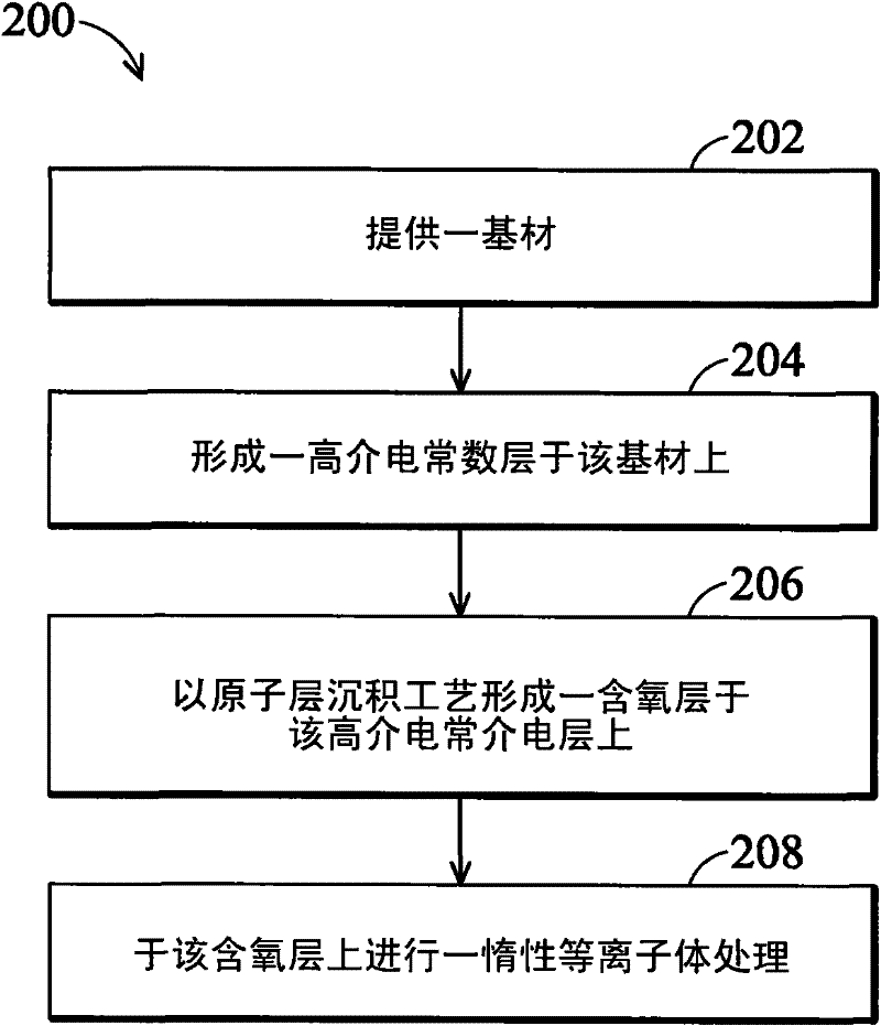
[0029] figure 2 A method 200 of fabricating the high-k gate dielectric layer 312 (shown in FIG. 3 ) in accordance with an embodiment of the present invention is shown. Figure 3A-Figure 3H A cross-sectional...


PUM

PropertyMeasurementUnit
thicknessaaaaaaaaaa
thicknessaaaaaaaaaa
thicknessaaaaaaaaaa

Abstract

A method for fabricating a gate dielectric layer comprises forming a high-k dielectric layer over a substrate; forming an oxygen-containing layer on the high-k dielectric layer by an atomic layer deposition process; and performing an inert plasma treatment on the oxygen-containing layer. The silicon oxide is prevented from being generated on the surface of the top of the substrate to keep the performance characteristics of the device.

Description

technical field [0001] The present invention relates to integrated circuit fabrication, and more particularly to a semiconductor device having a gate dielectric layer. Background technique [0002] The semiconductor integrated circuit (IC) industry has experienced rapid growth. Technological advances in IC materials and design have resulted in successive generations of IC production, each with smaller and more complex circuits than the previous generation. As the size of transistors shrinks, the thickness of the gate dielectric layer must be thinned as the gate channel length is reduced to maintain performance. However, in order to reduce the gate leakage current, it is necessary to use a high-k gate dielectric layer as the gate dielectric layer used in future advanced nodes, which can have a thicker physical thickness while maintaining the same equivalent thickness. [0003] Figure 1A and Figure 1B Cross-sectional views of the high-k gate dielectric layer 112 of a conv...

Claims


Application Information

Patent Timeline
Patent Type & Authority Applications(China)
IPC IPC(8): H01L21/283
CPCH01L21/02181H01L21/0228H01L21/02323H01L21/02337H01L21/0234H01L21/28194H01L29/495H01L29/4966H01L29/513H01L29/517H01L29/66545H01L29/6659
Inventor 李威养于雄飞陈建豪侯承浩李达元许光源
Owner TAIWAN SEMICON MFG CO LTD
Why Eureka
Try Eureka