Split-gate type memory and manufacturing method thereof

A technology of split-gate memory and manufacturing method, applied in semiconductor/solid-state device manufacturing, semiconductor devices, electrical components, etc., can solve the problems of improving the capacitive coupling rate, gate polysilicon residue, etc., and achieve the improvement of capacitive coupling rate, The effect of reducing erase voltage, increasing process cost and memory production cost

Active Publication Date: 2011-10-19
SHANGHAI HUAHONG GRACE SEMICON MFG CORP
View PDF8 Cites 0 Cited by
  • Summary
  • Abstract
  • Description
  • Claims
  • Application Information

AI Technical Summary

Problems solved by technology

[0009] However, the above method cannot improve the capacitive coupling ratio while avoiding gate polysilicon residue

Method used


Image

  • Split-gate type memory and manufacturing method thereof
  • Split-gate type memory and manufacturing method thereof
  • Split-gate type memory and manufacturing method thereof

Examples


Embodiment Construction

[0023] In order to make the content of the present invention clearer and easier to understand, the content of the present invention will be described in detail below in conjunction with specific embodiments and accompanying drawings.

[0024] figure 1 A flow chart of a method for manufacturing a split-gate memory according to an embodiment of the present invention is schematically shown.

[0025] like figure 1 As shown, the manufacturing method of split-gate memory according to the present invention includes:

[0026] First, a photolithography step S1 is performed to define shallow trench isolation regions. For the photolithography step S1, any suitable method known in the art may be used, which is not specifically limited in the present invention.

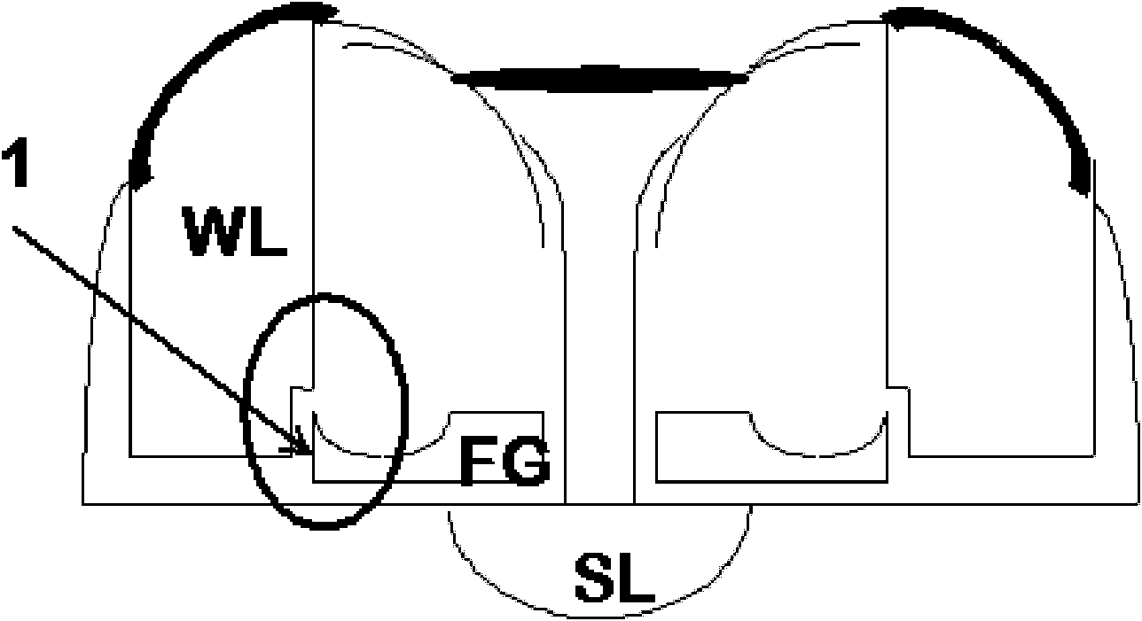
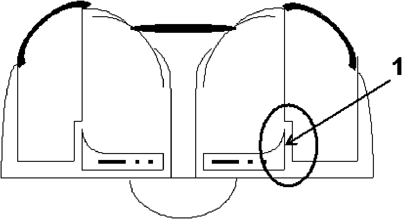
[0027] The shallow trench isolation area etching step S2 is then performed, wherein the height of the shallow trench isolation in the word line area of ​​the cell array of the split-gate memory is reduced, thereby preventing po...


PUM


Abstract

The invention provides a split-gate type memory and a manufacturing method thereof. According to the manufacturing method of the split-gate type memory, provided by the invention, the method comprises: a photoetching step for defining a shallow trench isolated region; a step for etching the shallow trench isolated region, wherein the height of the shallow trench isolated region of a word line region of a unit array in the split-gate type memory is reduced; a barrier layer removing step for removing the barrier layers of the regions not covered by photoresistance; a floating gate (FG) polysilicon etching step for etching floating gate polysilicon not covered by the photoresistance; and an FG and word line etching step for etching an FG and a word line. The height of the top end of the FG of the split-gate type memory manufactured according to the manufacturing method of the split-gate type memory, provided by the invention, is lowered, the capacitance between the FG and the word line is reduced, and the capacitance between the FG and a select line is maintained invariable, therefore, the capacitance coupling efficiency is accordingly reduced so as to be helpful to improving programming efficiency and reducing an erasing voltage.

Description

technical field [0001] The invention relates to a manufacturing method of a split-gate memory and a split-gate memory obtained by the method. Background technique [0002] With the development of semiconductor manufacturing technology, a split-gate flash memory having a control gate and a floating gate has been developed. In the flash memory, in order to save the space of the circuit layout and reduce the size of the memory device, usually, for example, every two bits share a source / drain for writing, reading and erasing operations. [0003] In the manufacture of flash memory, it has been proposed to use shallow trench isolation (shallow trench isolation, STI) isolation technology to replace the traditional local oxidation of silicon (LOCOS) to isolate the active region to achieve the purpose of reducing the size of the storage device. Thus, the integration degree of the semiconductor device is effectively improved. [0004] However, as the size of the memory device shrink...

Claims


Application Information

Patent Timeline
Patent Type & Authority Applications(China)
IPC IPC(8): H01L21/8247H01L21/336H01L29/788H01L29/423
Inventor 李冰寒孔蔚然江红
Owner SHANGHAI HUAHONG GRACE SEMICON MFG CORP
Why Eureka
Try Eureka