Ion implantation system and method

An ion implantation system and ion implantation technology, which are applied in the field of ion implantation systems, can solve problems such as design difficulties, and achieve the effects of convenient installation and debugging, ensuring implantation quality and reducing design size.

Active Publication Date: 2011-11-09
KINGSTONE SEMICONDUCTOR LIMITED COMPANY
View PDF3 Cites 11 Cited by
  • Summary
  • Abstract
  • Description
  • Claims
  • Application Information

AI Technical Summary

Problems solved by technology

[0006] The technical problem to be solved by the present invention is to overcome a series of design difficulties in the existing ion implantation system because the ion beam needs to be scanned by the scanning magnet in a large angle range, and to provide a system that can completely solve the above-mentioned series of designs. Difficult ion implantation systems and methods

Method used


Image

  • Ion implantation system and method
  • Ion implantation system and method
  • Ion implantation system and method

Examples


Embodiment 1

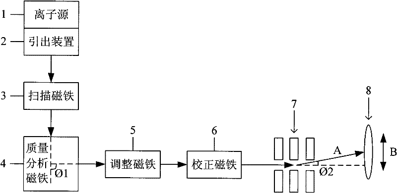
[0043] When the ion implantation system of the present invention is used to perform high-energy ion implantation, the figure 1 The shown beam transmission path transmits the ion beam to the implantation station, so as to finally complete the ion implantation process on the workpiece.

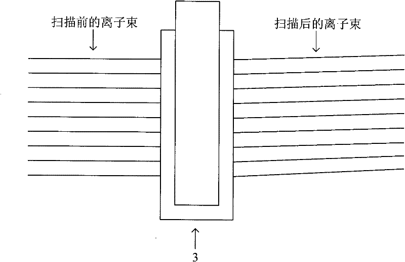
[0044] First, an ion beam is extracted from the ion source 1 by the extraction device 2 . Then pass through the scanning magnet 3 in the figure 1 The ion beam is scanned in a direction perpendicular to the paper, so that the ion beam forms a distribution in the scanning direction. Next, the ion beam passes through the mass analysis magnet 4 and is deflected by the mass analysis magnet 4 In this way, only ions suitable for implantation with energies within a preset range of charge-to-mass ratio remain in the beam after passing through the mass analysis magnet 4 . Wherein, in particular, the operating parameters of the mass analysis magnet 4 are set to: make the angle relatively small (less ...

Embodiment 2

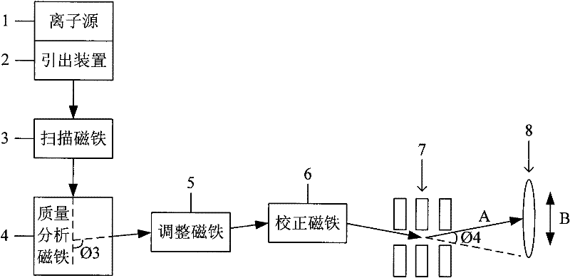
[0046] When the ion implantation system of the present invention is used to perform low-energy ion implantation, the figure 2 The shown beam transmission path transmits the ion beam to the implantation station, so as to finally complete the ion implantation process on the workpiece.

[0047] The only difference between the system in this embodiment and the system in Embodiment 1 is: at this time, the mass analysis magnet 4 performs a relatively large deflection angle on the beam current (more than the figure 1 middle ), that is, the beam current is deflected to cross the entrance of the speed change device 7, correspondingly, when the beam current reaches the correcting magnet 6, the beam current is deflected back to the direction aligned with the entrance of the speed change device 7 by the correction magnet 6. This rectifying magnet 6 that has correction and deflection effect simultaneously can utilize the magnet device of various existing structures to realize, but pre...


PUM


Abstract

The invention discloses an ion implantation system comprising an ion source and a leading-out device, wherein a scanning magnet, a mass analysis magnet, a correcting magnet, a speed changing device and a workpiece scanning device are arranged on a transmission path of an ion beam current in sequence; the system also comprises an adjusting magnet arranged on a beam current transmission path between the mass analysis magnet and the correcting magnet; and the adjusting magnet is used for diverging or gathering beam currents in the scanning direction. The invention also discloses an ion implantation method realized by using the ion implantation system. According to the invention, lower energy consumption and higher beam current utilization efficiency are obtained so that the production efficiency can be largely enhanced; in addition, the ion implantation system and method, disclosed by the invention, are also beneficial for optimizing the dose uniformity and the angle uniformity of the beam currents.

Description

technical field [0001] The invention relates to the field of semiconductor manufacturing, in particular to an ion implantation system and method. Background technique [0002] The ion implantation method is used to introduce atoms or molecules, usually called impurities, into the target substrate, thereby changing the properties of the substrate material. Ion implantation methods can be used to surface implant materials to alter their physical and chemical properties. [0003] Of particular interest is the doping of single or polycrystalline silicon by ion implantation, a routine process in the manufacture of modern integrated circuits. Since the production of semiconductor products gradually tends to larger semiconductor wafers (from 8 inches to 12 inches, and has now developed to 18 inches), the current single wafer process (processing one wafer at a time) has been widely used. The larger the wafer workpiece, the longer it takes to implant, and it becomes more and more d...

Claims


Application Information

Patent Timeline
Patent Type & Authority Applications(China)
IPC IPC(8): H01J37/317H01J37/32H01L21/265
Inventor 陈炯钱锋
Owner KINGSTONE SEMICONDUCTOR LIMITED COMPANY
Why Eureka
Try Eureka