Array substrate and manufacturing method thereof, and liquid crystal display
A manufacturing method and array substrate technology, applied in semiconductor/solid-state device manufacturing, instruments, electric solid-state devices, etc., can solve the problems of increasing the number of mask patterning processes, reducing production efficiency, and complicated processes, so as to simplify the production process, The effect of small data line spacing and efficient preparation of array substrates
- Summary
- Abstract
- Description
- Claims
- Application Information
AI Technical Summary
Problems solved by technology
Method used
Image

Examples
Embodiment 1
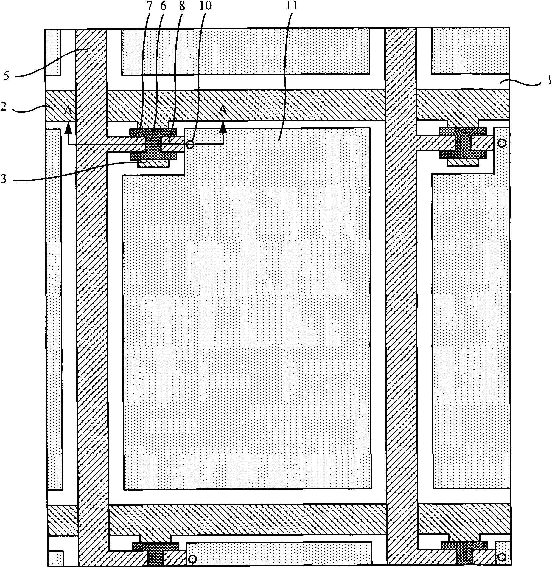
[0040] image 3 The flow chart of the manufacturing method of the array substrate provided in Embodiment 1 of the present invention, the manufacturing method includes the process of forming gate lines, gate electrodes, active layers, data lines, source electrodes, drain electrodes and pixel electrode patterns in the pixel area and simultaneously The process of forming gate lines and data line patterns in the interface area, the method of this embodiment is specifically a method for preparing an array substrate using a four-time mask patterning process, including the following steps:
[0041] Step 301, depositing a gate metal thin film on the base substrate 1, using a monotone mask, etching the gate metal thin film through a patterning process to form a pattern including gate lines 2 and gate electrodes 3; the gate metal thin film can be made of a non-transparent Made of photoconductive materials, such as aluminum, neodymium, molybdenum and other metals.
[0042] Step 302: For...
Embodiment 2
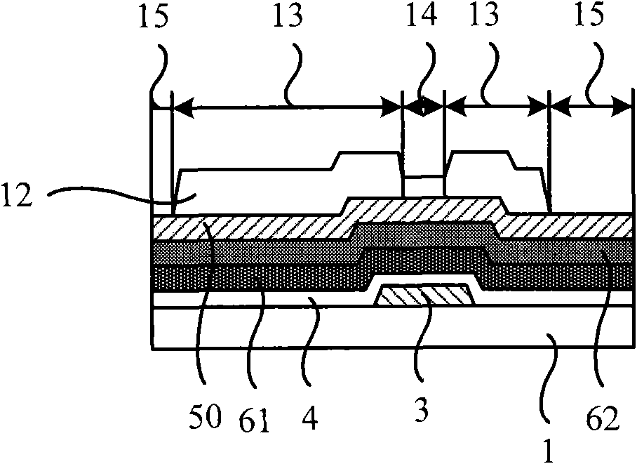
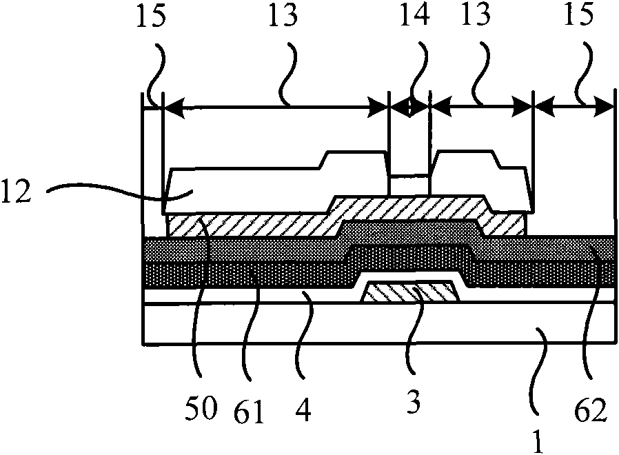
[0060] Figure 8 It is a partial flow chart of the manufacturing method of the array substrate provided in Embodiment 2 of the present invention. Through the patterning process, the passivation layer film above the drain electrode is etched away to form the pattern of the passivation layer via hole, and the interface is etched away at the same time. The specific steps for the passivation layer film and the remaining active layer film corresponding to the part of the reserved area in the region are as follows:
[0061] A two-tone mask is used for the patterning process, and the passivation layer film above the drain electrode is etched by the first etching to form a passivation layer via hole pattern, and then etched by the second etching The passivation layer film and the remaining active layer film corresponding to the part of the reserved area in the interface area include the following steps:
[0062] Step 801, forming a passivation layer film 90 on the base substrate 1 af...
PUM
 Abstract
Description
Claims
Application Information
 - R&D
- Intellectual Property
- Life Sciences
- Materials
- Tech Scout
- Unparalleled Data Quality
- Higher Quality Content
- 60% Fewer Hallucinations
Browse by: Latest US Patents, China's latest patents, Technical Efficacy Thesaurus, Application Domain, Technology Topic, Popular Technical Reports.
© 2025 PatSnap. All rights reserved.Legal|Privacy policy|Modern Slavery Act Transparency Statement|Sitemap|About US| Contact US: help@patsnap.com