Avalanche photodiode

An avalanche photoelectric, diode technology, applied in circuits, electrical components, semiconductor devices, etc.

Inactive Publication Date: 2011-11-23
ALCATEL LUCENT SAS
View PDF2 Cites 15 Cited by
  • Summary
  • Abstract
  • Description
  • Claims
  • Application Information

AI Technical Summary

Problems solved by technology

However, very thin transition layers (consisting of graded and charge layers) lead to undesired multiplication in the absorbing region

Method used


Image

  • Avalanche photodiode
  • Avalanche photodiode
  • Avalanche photodiode

Examples


Embodiment Construction

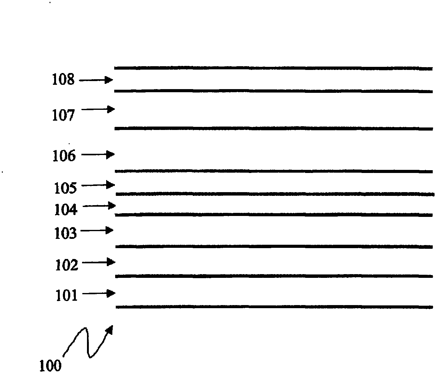
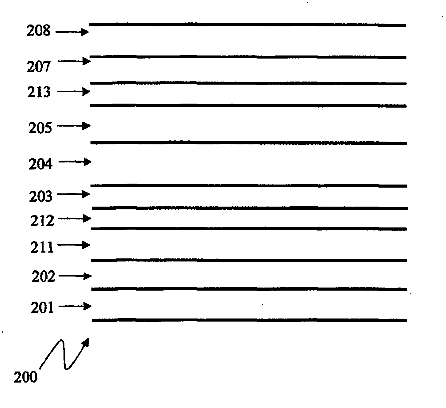
[0022] To better understand the structure of the APD proposed in this paper, some known APD structures are first referred to.

[0023] A first example is an APD structure comprising an avalanche layer made of bulk AlInAs material or AlInAs / AlGaInAs MQW (Multiple Quantum Wells) and an absorber layer made of GaInAs material. The bulk multiplication layer is made thin enough to allow a large ionization coefficient ratio k, where k=α / β, α and β are the ionization coefficients of electrons and holes, respectively, by reducing the fluctuation of the multiplication events. This results in reduced excess noise and improved gain-bandwidth product. By using waveguides for lateral illumination and very thin absorbing layers (about 0.5 μm) and multiplication layers (about 0.1 μm), the APD exhibits a 3dB bandwidth of 30 GHz at low gain and a limited gain-bandwidth product of 140 GHz. This is not a satisfactory result because for high speed operation at 40Gb / s, this low gain-bandwidth prod...


PUM


Abstract

A single carrier avalanche photodiode (200) comprising a p-doped absorption layer (213), an unintentionally doped avalanche multiplication layer (203) and an n-doped collector layer (211) and a method of manufacturing said avalanche photodiode. The absorption layer is doped at a level that allows the photodiode to operate as a single carrier device. Therefore total delay time of the device is mainly dependent on electrons. The collector layer is in charge of reducing capacitance in the device. A built-in field layer (212) of n plus delta doped material may be provided between the two layers in order to improve the injection of electrons in the collector layer.

Description

technical field [0001] The present invention relates to avalanche photodiodes. Background technique [0002] Avalanche photodiodes (APDs) are widely used as components in various telecommunication applications such as fiber optic optical transmission systems, free-space optical communications, and other optical applications such as high-resolution ranging, sensing, spectroscopy, etc., because avalanche The internal gain of the diode (APD) significantly increases the sensitivity of the photoreceiver for specific applications. Currently, APDs are used to increase the power budget for channel data rates below 10Gb / s. However, it is likely that some similar pathways have led to the deployment of high-speed networks with data rates at or above 10 Gb / s that currently operate using pin receivers. The expected significant increase in sensitivity (expected up to about 10 dB) may indeed allow the replacement of expensive gain-blocking elements such as Erbium-doped fiber amplifiers (...

Claims


Application Information

Patent Timeline
Patent Type & Authority Applications(China)
IPC IPC(8): H01L31/107H01L31/0304
CPCH01L31/1075H01L31/03046H01L31/107
Inventor 莫昂·阿舒什
Owner ALCATEL LUCENT SAS
Why Eureka
Try Eureka