Sonos structure and its production method
A manufacturing method and curved surface technology, applied in electrical components, circuits, semiconductor devices, etc., can solve problems such as unclean erasing, and achieve the effect of enhancing the speed, reducing the speed, and solving the problem of erasing saturation.
- Summary
- Abstract
- Description
- Claims
- Application Information
AI Technical Summary
Problems solved by technology
Method used
Image

Examples
Embodiment Construction
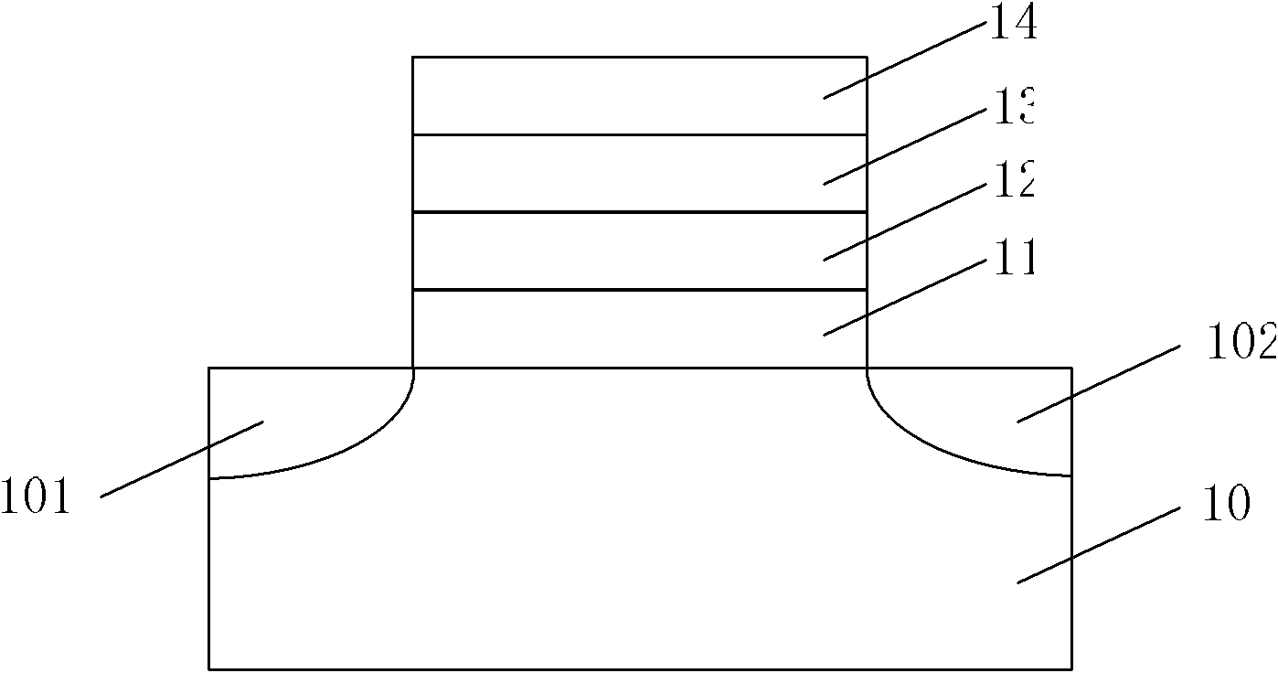
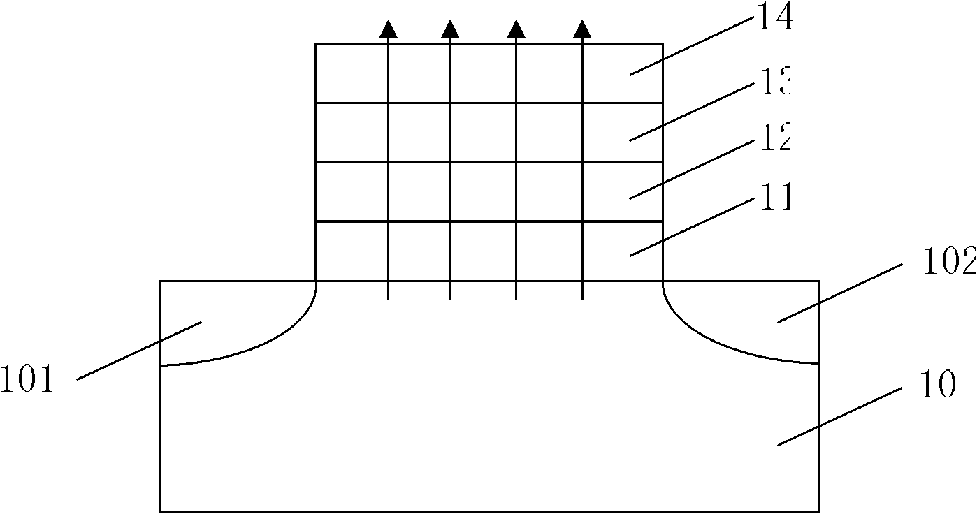
[0035] As mentioned in the background art, figure 1 The shown SONOS structure often exhibits erase saturation during use. The inventor of the present invention analyzes that during the erase process, electrons stored in the nitride layer 12 are under the action of the electric field generated by the reverse voltage of the polysilicon layer 14. Such as figure 2 As shown, the first oxide layer 11 enters the substrate 10; however, the electrons in the polysilicon layer 14 will pass through the second oxide layer 13 and enter the nitride layer 12 under the action of the electric field generated by the counter voltage. When the rate of entering the nitride layer 12 is equal to the rate of flowing out of the nitride layer 12, the erasing saturation is reached. At this time, there are still electrons stored in the nitride layer 12, so it is difficult to erase cleanly.
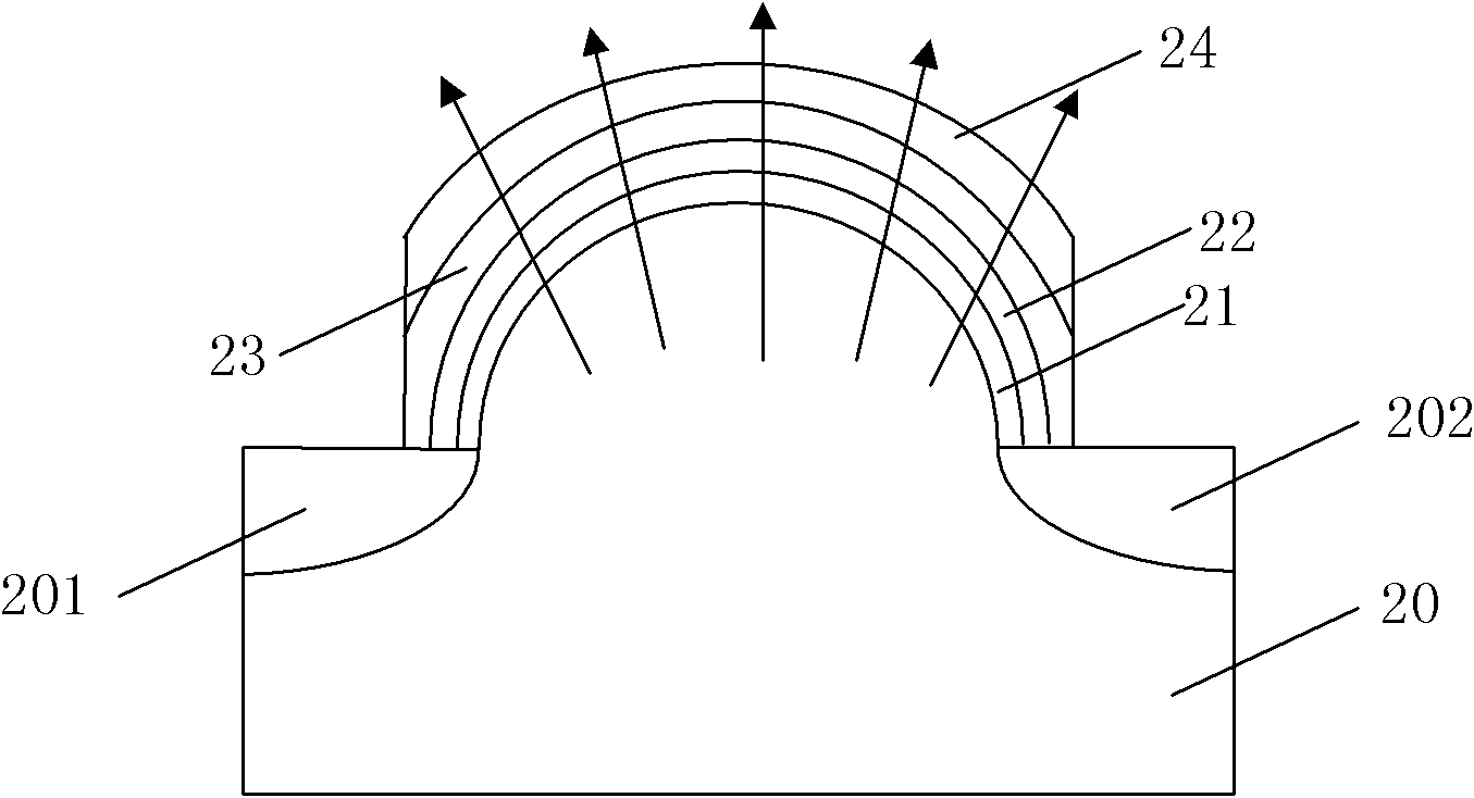
[0036] In order to overcome the fact that the rate of electrons entering the nitride layer 12 is equal to the rate of ...
PUM
 Abstract
Description
Claims
Application Information
 - R&D
- Intellectual Property
- Life Sciences
- Materials
- Tech Scout
- Unparalleled Data Quality
- Higher Quality Content
- 60% Fewer Hallucinations
Browse by: Latest US Patents, China's latest patents, Technical Efficacy Thesaurus, Application Domain, Technology Topic, Popular Technical Reports.
© 2025 PatSnap. All rights reserved.Legal|Privacy policy|Modern Slavery Act Transparency Statement|Sitemap|About US| Contact US: help@patsnap.com