Supercharge Your Innovation With Domain-Expert AI Agents!

Sonos structure and its production method

A manufacturing method and surface-shaped technology, which is applied in the direction of electrical components, circuits, semiconductor devices, etc., can solve the problem of unclean erasing, achieve the effect of increasing the rate, reducing the rate, and solving the problem of erasing saturation

Active Publication Date: 2015-11-11
SHANGHAI HUAHONG GRACE SEMICON MFG CORP
View PDF5 Cites 0 Cited by
  • Summary
  • Abstract
  • Description
  • Claims
  • Application Information

AI Technical Summary

Problems solved by technology

[0004] However, during the use of this SONOS structure, the phenomenon of erase saturation often occurs, that is, the problem of unclean erase

Method used


Image

  • Sonos structure and its production method
  • Sonos structure and its production method
  • Sonos structure and its production method

Examples


Embodiment Construction

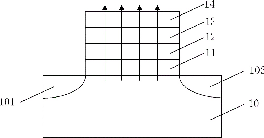
[0035] As mentioned in the background art, figure 1 The SONOS structure shown often appears erase saturation phenomenon during use. The inventors of the present invention analyze that during the erasing process, the electrons stored in the nitride layer 12 are under the action of the electric field generated by the reverse voltage of the polysilicon layer 14. Such as figure 2 As shown, the electrons in the polysilicon layer 14 enter the substrate 10 through the first oxide layer 11; however, the electrons in the polysilicon layer 14 will pass through the second oxide layer 13 and enter the nitride layer 12 under the action of the electric field generated by its reverse voltage, when the electrons When the rate of entering the nitride layer 12 is equal to the rate of flowing out of the nitride layer 12, the erasing saturation is reached. At this time, there are still electrons stored in the nitride layer 12, so it is difficult to erase completely.

[0036] In order to overcom...


PUM


Abstract

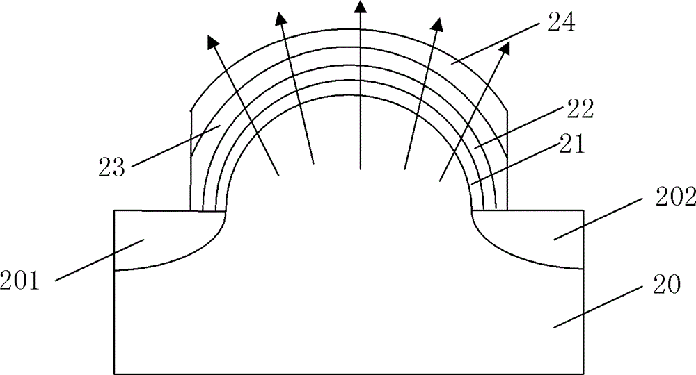
The invention provides a SONOS structure, comprising: a silicon semiconductor substrate containing silicon curved surface protrusions, an active region and a drain region are formed in adjacent regions of the silicon curved surface protrusions; the silicon curved surface protrusions are sequentially formed with the first One oxide layer, nitride layer, second oxide layer, polysilicon layer. The invention also provides a manufacturing method of the SONOS structure. By adopting the SONOS structure provided by the present invention, the erasing saturation phenomenon can be avoided during use.

Description

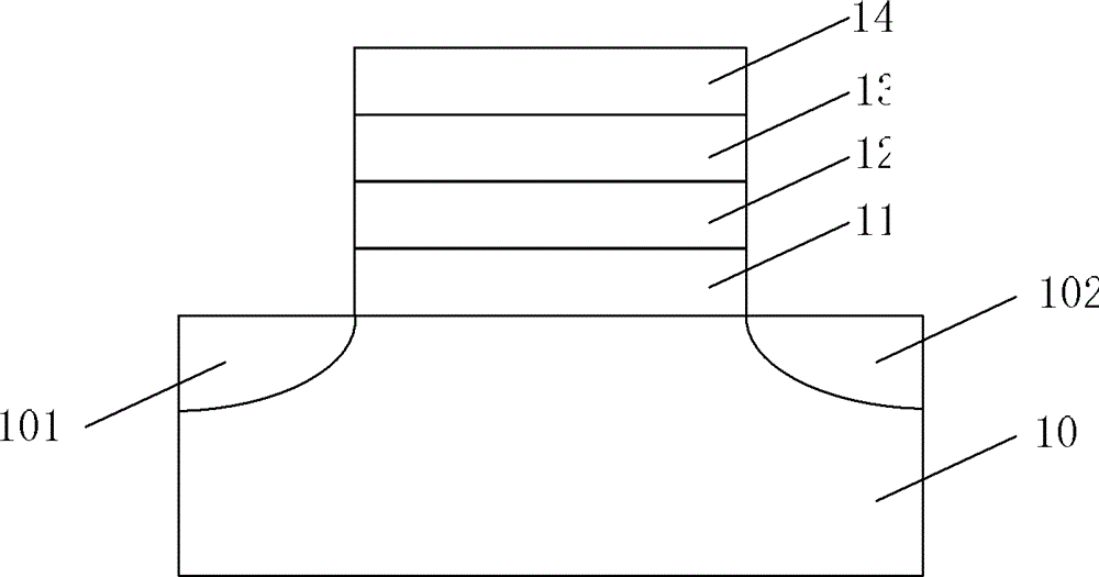
technical field [0001] The invention relates to the field of semiconductor manufacturing, in particular to a SONOS structure and a manufacturing method thereof. Background technique [0002] Random access memory, such as DRAM and SRAM, has the problem of data loss after power failure during use. To overcome this problem, various nonvolatile memories have been designed and developed. For example a silicon-oxide-nitride-oxide-silicon (SONOS) structure. [0003] figure 1 It is an existing SONOS structure, comprising: a silicon substrate 10, forming a first oxide layer 11, a nitride layer 12, a second oxide layer 13, a polysilicon layer 14 as a gate and forming a silicon substrate 10 stacked in sequence A source region 101 and a drain region 102 in the silicon substrate 10 . SONOS structure, such as NMOS, the writing process is: V GS greater than the turn-on voltage, when the drain region 102 and the source region 101 form a positive voltage drop, the hot carrier jumps thro...

Claims


Application Information

Patent Timeline
Patent Type & Authority Patents(China)
IPC IPC(8): H01L21/28H01L29/423
Inventor 苟鸿雁吴小利唐树澍
Owner SHANGHAI HUAHONG GRACE SEMICON MFG CORP
Features
  • R&D
  • Intellectual Property
  • Life Sciences
  • Materials
  • Tech Scout
  • Unparalleled Data Quality
  • Higher Quality Content
  • 60% Fewer Hallucinations
Learn More