Data input and output control device and semiconductor storage device system
A storage device, input and output technology, applied in the direction of digital memory information, information storage, static memory, etc., can solve the problems of increased power consumption of error correction circuits, uncorrectable errors, and increased processing time.
- Summary
- Abstract
- Description
- Claims
- Application Information
AI Technical Summary
Problems solved by technology
Method used
Image
Examples
Embodiment Construction
[0054] Next, the best embodiment of the present invention will be explained with examples.
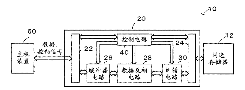
[0055] figure 1 It is a schematic configuration diagram of the configuration of the flash memory system 10 equipped with the data input / output control device as the first embodiment of the present invention. The flash memory system 10 is composed of a flash memory 12 formed by stacking a plurality of silicon chips formed with NAND flash memory and a memory controller 20 that controls the flash memory 12, and a host device 60 (for example, a personal computer) It is communicatively connected, and according to various control signals input from the host device 60, the data input from the host device 60 is stored in the flash memory 12 or the data stored in the flash memory 12 is output to the host device 60. In addition, such flash memory 12 and memory controller 20 are formed on mutually different semiconductor chips.
[0056] The flash memory 12 is configured to include a flash memory cell...
PUM
 Abstract
Description
Claims
Application Information


