Soc integrated circuit with multiplexing of functional interface and debugging interface
A technology of integrated circuit and debugging interface, which is applied in the direction of electrical digital data processing, instruments, digital data processing components, etc., and can solve problems such as uncertain factors, inability to debug, and long time consumption
- Summary
- Abstract
- Description
- Claims
- Application Information
AI Technical Summary
Problems solved by technology
Method used
Image
Examples
Embodiment 1
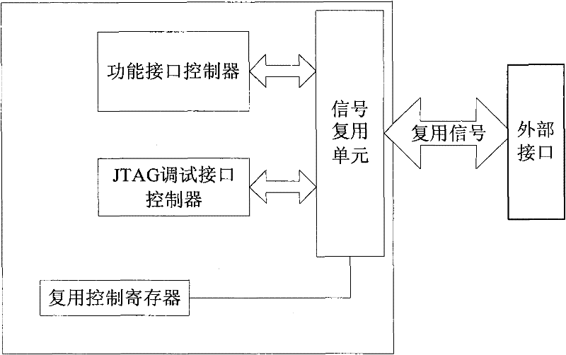
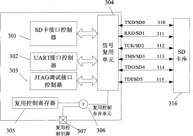
[0025] Such as image 3 as shown, image 3 It is a schematic structural diagram of an SOC integrated circuit applied to SD card control in this embodiment. In the figure, SOC 300 includes: SD card interface controller 301, UART interface controller 302, JTAG debug interface controller 303, signal multiplexing unit 304, multiplexing control register 305, multiplexing control merging unit 306, multiplexing control pipe pin 307 , pins 310 to 315 , and SD card socket 316 . Wherein the SD card interface controller 301, i.e. the secure digital card interface controller, corresponds to figure 2 The main function of the functional interface controller is to realize the read and write operation of the externally inserted SD card and realize the function of SD card storage. This is a functional application in normal mode; the UART interface controller 302 corresponds to figure 2 Other debugging interface controllers in the UART are used to communicate with external debugging tools ...
Embodiment 2
[0029] Figure 4 Shown is a schematic diagram of the structure of the SOC integrated circuit used in MS card control. The SOC integrated circuit in the figure includes: MS interface controller 401, JTAG debugging interface controller 403, multiplexing control register 405, signal multiplexing unit 404, pins 410-415, and MS external socket 416. where the MS interface controller 401 corresponds to figure 2 The function interface controller, its main function is to realize the data storage of the externally inserted MS card. This implementation is a simplified version without image 3 The multiplexing control pin 307 shown in , because there is only a single control mode, does not need the multiplexing control merging unit 306; figure 2 Other debug interface controllers shown in .
[0030] During normal function application: the multiplexing control register 405 does not receive the debug mode trigger command, and then outputs the normal application control command to contr...
PUM
 Abstract
Description
Claims
Application Information


