field emission display device

A display device and field emission technology, applied in image/graphic display tubes, cathode ray tubes/electron beam tubes, discharge tubes, etc., can solve problems such as deflection, field emission source damage to electrons, etc., to simplify the cathode structure and improve The uniformity of electron emission and the effect of avoiding damage

Inactive Publication Date: 2011-12-21
CPT DISPLAY TECH FUJIAN +1
View PDF2 Cites 0 Cited by
  • Summary
  • Abstract
  • Description
  • Claims
  • Application Information

AI Technical Summary

Problems solved by technology

However, in the manufacturing process, the field emission source is easily damaged by the external structure on the cathode substrate, or electronic deflection occurs. Therefore, how to improve the uniformity of electron emission while avoiding damage to the field emission source has become a research topic. research goals

Method used


Image

  • field emission display device
  • field emission display device
  • field emission display device

Examples


Embodiment Construction

[0020] In order to make the object, technical solution and advantages of the present invention clearer, the present invention will be further described in detail below through specific embodiments and related drawings.

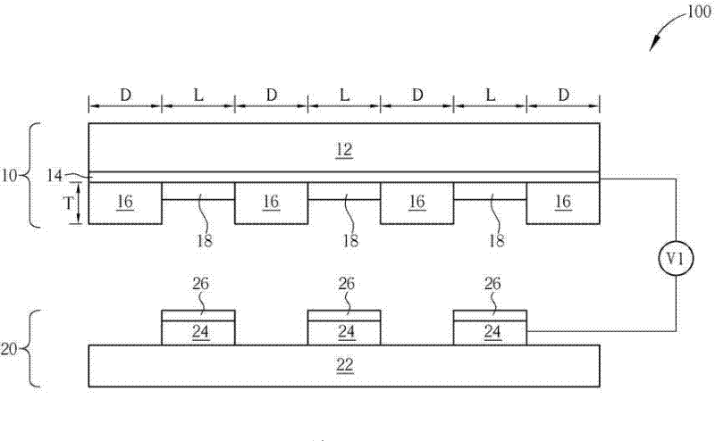
[0021] Please refer to figure 1 , figure 1 It is a schematic diagram of the field emission display device according to the first embodiment of the present invention. Such as figure 1 As shown, the field emission display device 100 of the first embodiment of the present invention includes an anode structure 10 and a cathode structure 20 . The anode structure 10 includes an anode substrate 12 , an anode layer 14 , a plurality of dielectric patterns 16 and a plurality of light emitting patterns 18 . In this embodiment, a plurality of dielectric regions D and a plurality of light emitting regions L are defined on the anode substrate 12 . The anode layer 14 is located on the anode substrate 12, and the anode layer 14 may include a transparent electrode laye...


PUM


Abstract

The invention provides a field emission display device, which includes an anode structure and a cathode structure oppositely arranged. The anode structure includes an anode substrate, an anode layer, a plurality of dielectric patterns and a plurality of light emitting patterns. The cathode structure includes a cathode substrate facing the anode substrate, a plurality of cathode patterns and a plurality of field emission sources, wherein each field emission source corresponds to each light emitting pattern of the anode structure. In the field emission display proposed by the present invention, the dielectric pattern in the anode structure can cause the distortion of the potential line, so that the local electric field at the edge of the dielectric pattern can be enhanced to attract electrons emitted by the field emission source, so the uniformity of electron emission can be effectively improved . In addition, because the invention has a simplified cathode structure, the field emission source can be prevented from being damaged during the manufacturing process.

Description

technical field [0001] The invention relates to a field emission display, in particular to a field emission display which can improve the uniformity of electron emission and prevent the field emission source from being damaged during the manufacturing process. [0002] Background technique [0003] Field emission display is the next-generation emerging technology with the most development potential after cathode ray tube display and liquid crystal display. Compared with the existing display technology, the field emission display has the advantages of low driving voltage, no viewing angle limitation, wide operating temperature range, high brightness, high contrast and color saturation, etc., especially the carbon nanotube field emission display, which has become more and more popular in recent years. more attention. [0004] [0005] Generally speaking, a field emission display includes an anode substrate coated with a fluorescent material and a cathode substrate provided ...

Claims


Application Information

Patent Timeline
Patent Type & Authority Applications(China)
IPC IPC(8): H01J31/12H01J29/08
Inventor 江美昭李怀安蔡五湖黄彦余
Owner CPT DISPLAY TECH FUJIAN
Why Eureka
Try Eureka