Method for reducing carbon nanotube loss when sealing and joining field emission display device

A technology of carbon nanotubes and display devices, which is applied in the manufacture of discharge tubes/lamps, electrical components, ships or lead wires, etc. It can solve the problems of uneven cathode emission, affecting the service life of devices, and short service life. Achieve the effects of reducing carbon nanotube loss, improving emission uniformity, and reducing blowing effect

Inactive Publication Date: 2010-01-13
SOUTHEAST UNIV
View PDF2 Cites 0 Cited by
  • Summary
  • Abstract
  • Description
  • Claims
  • Application Information

AI Technical Summary

Problems solved by technology

In this way, under the action of the same electric field between the cathode and the anode, it directly leads to uneven emission of the cathode, where the carbon nanotubes are more distributed, the emission is stronger, where the carbon nanotubes are less distributed, the emission is weaker, and where there are no carbon nanotubes. There is no emission in the place, which cannot solve the uniformity of the display of the device; similarly, due to the loss of carbon nanotubes, it will also affect the service life of the device
Therefore, the loss of carbon nanotubes during the heating process of carbon nanotube field emission display devices (CNT-FEDs) is the main reason for the uneven emission and short service life of the device.

Method used


Image

  • Method for reducing carbon nanotube loss when sealing and joining field emission display device
  • Method for reducing carbon nanotube loss when sealing and joining field emission display device

Examples


Embodiment Construction

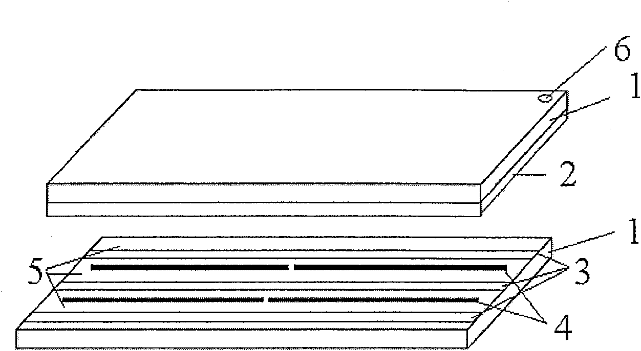
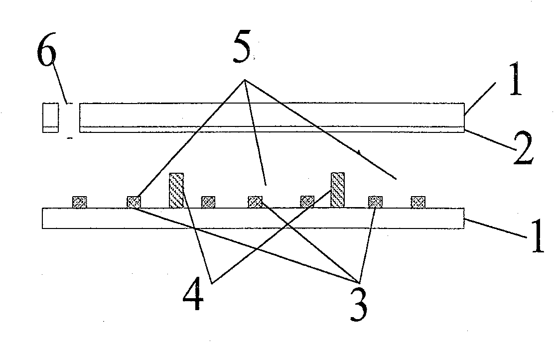
[0011] The method that reduces carbon nanotube field emission display device (CNT-FEDs) of the present invention and carbon nanotube is lost in sealing process is applied in the field emission display of 5 inches, in carbon nanotube field emission display device (CNT-FEDs ) During the sealing process, an insulating dielectric strip 4 with a length of 8-12 centimeters, a width of 0.2-0.5 millimeters and a thickness of 40-80 microns made by screen printing is printed between two adjacent cathodes 3, The vacuum sealing cavity is evenly divided into 3-20 small vacuum cavities 5 with an insulating dielectric strip 4, and the insulating dielectric strip 4 is made of SiO 1 (CH 2 CH 3 ) 2 Materials are printed. The small vacuum chambers 5 communicate with each other by leaving a gap of 0.6-1.2 centimeters between the two ends and the middle of the insulating dielectric strip 4, as the exhaust channels of each chamber, forming a new type of carbon nanotube field emission display dev...


PUM

PropertyMeasurementUnit
lengthaaaaaaaaaa
widthaaaaaaaaaa
thicknessaaaaaaaaaa

Abstract

The invention discloses a carbon nanometer pipe field launching displaying element losing avoiding method in the sealing carbon nanometer pipe, which comprises the following steps: adopting silk screen printing method as insulating dielectric between two adjacent cathodes in the carbon nanometer pipe field launching displaying element; dividing vacuum sealing cavity into less cavities evenly with gap interconnecting through insulating dielectric heads and middle as vent channel for each cavity; forming a new sealing structure of new typed carbon nanometer pipe field launching displaying element; sealing the element to reduce countercurrent degree for gas in the sealing cavity; reducing blowing action of carbon nanometer pipe by countercurrent gas; remaining large part of carbon nanometer pipe on the cathode.

Description

technical field [0001] The invention relates to a carbon nanotube display device, especially a large-size, high-brightness carbon nanotube display device (CNT-FEDs) that uses screen printing to reduce the loss of carbon nanotubes and reduce its impact on carbon nanotube field emission during the sealing process. Production process technology showing the impact of device emission uniformity. Background technique [0002] The display principle of field emission display devices (Field Emission Display, FEDs) is very close to that of traditional CRTs. FED has the advantages of high image quality of CRT and thin profile and low power consumption of LCD. It is considered as the best successor of CRT and has received widespread attention. And because carbon nanotubes have high mechanical strength, good chemical stability and high aspect ratio (>100), so sufficient field emission current, low turn-on field strength and large current density can be obtained in field emission , A...

Claims


Application Information

Patent Timeline
Patent Type & Authority Patents(China)
IPC IPC(8): H01J9/24H01J9/26H01J9/32H01J9/00
Inventor 崔云康张晓兵雷威狄云松王金蝉储开荣
Owner SOUTHEAST UNIV
Why Eureka
Try Eureka