A laser scanning annealing method using a hexagonal beam spot

A laser scanning and hexagonal technology, applied in the direction of electrical components, semiconductor/solid-state device manufacturing, circuits, etc., can solve the problems of process deviation and insufficient precision of mechanical control system, so as to improve the uniformity of the whole chip, reduce the realization cost, The effect of reducing the difficulty of implementation

Inactive Publication Date: 2011-12-21
TSINGHUA UNIV
View PDF5 Cites 4 Cited by
  • Summary
  • Abstract
  • Description
  • Claims
  • Application Information

AI Technical Summary

Problems solved by technology

Even if the precision of the mechanical control system of the wafer stage or laser beam scanning is not enough, for example, the overlapping area of ​​the two laser beams is only 90 micron

Method used


Image

  • A laser scanning annealing method using a hexagonal beam spot
  • A laser scanning annealing method using a hexagonal beam spot
  • A laser scanning annealing method using a hexagonal beam spot

Examples


Embodiment Construction

[0015] The invention provides a method for performing laser scanning annealing by using a hexagonal laser beam spot. Be described below in conjunction with accompanying drawing.

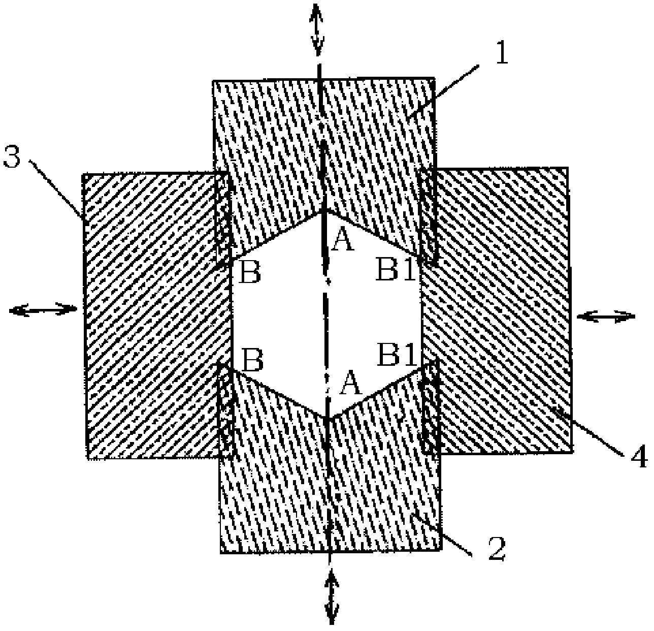
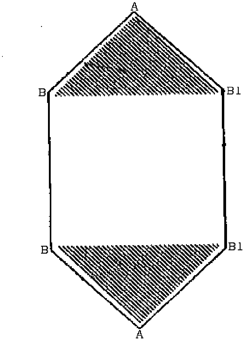
[0016] figure 1 Shown is a schematic diagram of the four-baffle mechanism forming a hexagonal beam spot. In the figure, the hexagonal laser beam spot, in the simplest case, is realized by four optical path baffles placed opposite each other in the optical path, that is, the baffle 1 and the baffle 2 are independent or move synchronously; the baffle 3 and the baffle 4 move independently or synchronously, and the four are all rectangular baffles, of which the upper baffle 1 and the lower baffle 2 or the opposite side of the left baffle 3 and the right baffle 4 , each opening a V-shaped opening to form a hexagonal vertex A, and the apex of the vertex A is on the center line; therefore, after the expanded and uniform laser beam passes through the baffle mechanism, the beam spot is hexagonal ABBAB1B1 ;...


PUM


Abstract

The invention discloses a laser scanning annealing method adopting a hexagonal beam spot, belonging to the semiconductor manufacturing technology. The hexagonal beam spot is formed by four baffle mechanisms capable of moving independently, each two of baffle mechanisms are arranged in an opposite way in an optical path, and an upper baffle and a lower baffle move independently or synchronously; and a left baffle and a right baffle move independently or synchronously, the four baffles all adopt rectangular baffles, the opposite sides of the upper baffle and the lower baffle or the left baffle and the right baffle are respectively provided with a V-shaped opening to form vertex angles A of a hexagon, and the vertexes of the vertex angles A are arranged on a central line. During wafer scanning annealing through the hexagonal beam spot, two adjacent scanning lines are overlapped for compensation, the problems of excessive or insufficient scanning between lines in the traditional line-by-line scanning can be solved, and the difficulty in implementation and the cost of implementation of the whole system cannot be increased.

Description

technical field [0001] The invention belongs to the technical field of semiconductor manufacturing, and particularly relates to a method for performing laser sweep annealing by using a hexagonal beam spot. Background technique [0002] In the development process of integrated circuit manufacturing technology, as the device size continues to shrink, how to form an ultra-shallow junction (Ultra-Shallow Junction) in the source and drain regions of transistors with excellent performance at technology nodes such as 45nm and 32nm, and even smaller sizes ), becoming a crucial technical challenge. In order to meet the requirements for ultra-shallow PN junction fabrication of 45nm and below-generation devices on 12″ wafers, the traditional light rapid thermal annealing (RTA) using strip or spherical lamps as light sources can no longer meet the requirements of ultra-shallow junctions. A large number of studies have shown that in nanoscale CMOS devices, ultra-shallow and low-resistiv...

Claims


Application Information

Patent Timeline
IPC IPC(8): H01L21/268
Inventor 刘朋严利人周卫窦维治刘志弘
Owner TSINGHUA UNIV
Why Eureka
Try Eureka