A hole-slit double-bridge acceleration sensor chip and its preparation method

An acceleration sensor, bridge-type technology, applied in the direction of acceleration measurement using inertial force, manufacturing microstructure devices, decorative arts, etc.

Inactive Publication Date: 2011-12-28
XI AN JIAOTONG UNIV
View PDF5 Cites 15 Cited by
  • Summary
  • Abstract
  • Description
  • Claims
  • Application Information

AI Technical Summary

Problems solved by technology

[0003] However, with the rapid development of micro-electromechanical system technology, the classic chip structure developed in the early stage has gradually been unable to meet and adapt to the requirements of high sensitivity and high res

Method used


Image

  • A hole-slit double-bridge acceleration sensor chip and its preparation method
  • A hole-slit double-bridge acceleration sensor chip and its preparation method
  • A hole-slit double-bridge acceleration sensor chip and its preparation method

Examples


Embodiment Construction

[0027] The present invention will be described in more detail below in conjunction with the accompanying drawings.

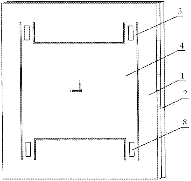
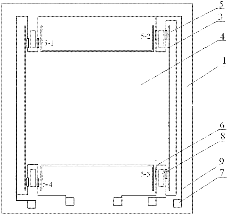
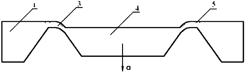
[0028] refer to figure 1 and figure 2 , a hole-slit double-bridge type acceleration sensor chip, including a silicon substrate 1 and a glass substrate 2 bonded to the back of the silicon substrate 1, a mass block 4 is arranged in the central cavity of the silicon substrate 1, and four open-hole sensitive beams One end of 3 is connected to the four corners of mass block 4, and the other end is connected to silicon substrate 1. A stress concentration hole 8 is provided in the center of each opening sensitive beam 3, and two stress concentration holes 8 are arranged on both sides of each stress concentration hole 8. Varistor strips, two varistor strips form a varistor 5, the first varistor 5-1 and the third varistor 5-3 of the four varistors 5 are arranged on the opening sensitive beam 3 The part connected with the quality block 4, the second piezoresistor 5-2 a...


PUM


Abstract

The invention discloses a hole-crack double-bridge type acceleration sensor chip and a preparation method thereof. The chip comprises a silicon substrate and a glass substrate bonded at back of the silicon substrate. A mass block is configured in a central empty cavity of the silicon substrate. One ends of four opening sensitive beams are connected with four corners of the mass block. The other ends of the four opening sensitive beams are connected with the silicon substrate. A stress concentration hole is arranged on each opening sensitive beam. Two piezoresistor strips are arranged at two sides of each stress concentration hole and form a piezoresistor. Four piezoresistors are connected through a metal lead wire and form a half open-loop Wheatstone full-bridge circuit. The four piezoresistors are simultaneously connected with five metal welding plates. The preparation method comprises the steps of obtaining the mass block in the silicon substrate and the opening sensitive beams through silicon anisotropic wet etching and ICP (Inductively Coupled Plasma) plasma etching and manufacturing the metal lead wire by adopting a titanium-platinum-gold multi-layer lead wire technology. Thestatic and dynamic sensitivity of the sensor can be increased by the chip. The chip has the advantages of small volume, low weight, high frequency response and high sensitivity.

Description

technical field [0001] The invention relates to an acceleration sensor chip, in particular to a hole-slit double-bridge type acceleration sensor chip and a preparation method thereof. Background technique [0002] As the earliest developed micro-acceleration sensor, the piezoresistive acceleration sensor has undergone long-term development and improvement, and has formed many classic structures, including single cantilever beam, double cantilever beam, four-beam, double-bridge and five-beam structures. The sensor chips of these structures all use micromachining technology to form a beam-island structure, and use piezoresistive effect to detect acceleration. In the single cantilever beam and double cantilever beam structure, the mass block freely swings up and down. The sensor chip of this type of structure has high sensitivity, but the natural frequency is low, the frequency response range is narrow, and the lateral sensitivity is relatively large. The single bridge, double...

Claims


Application Information

Patent Timeline
IPC IPC(8): G01P15/12B81C1/00
Inventor 赵玉龙孙禄刘岩田边蒋庄德
Owner XI AN JIAOTONG UNIV
Why Eureka
Try Eureka