An acceleration sensor chip with a composite multi-beam structure and its manufacturing method

An acceleration sensor and beam structure technology, applied in the direction of acceleration measurement using inertial force, microstructure technology, microstructure device, etc., can solve the problems of dynamic measurement of vibration acceleration, reduce the reliability of the sensor, and reduce the output of the sensor, etc., to achieve Facilitate cost reduction, anti-corrosion bonding properties, and good bonding properties

Inactive Publication Date: 2011-12-28
XI AN JIAOTONG UNIV
View PDF5 Cites 31 Cited by
  • Summary
  • Abstract
  • Description
  • Claims
  • Application Information

AI Technical Summary

Problems solved by technology

In order to use a single acceleration sensor to accurately identify the magnitude of acceleration and its frequency composition in different environments, the acceleration sensor used must have a sufficiently high response frequency and sensitivity at the same time. However, the response frequency and measurement sensitivity of the acceleration sensor are a set of interactions. Constrained parameters, increasing the response frequency will reduce the output of the sensor caused by the unit input acceleration

Method used


Image

  • An acceleration sensor chip with a composite multi-beam structure and its manufacturing method
  • An acceleration sensor chip with a composite multi-beam structure and its manufacturing method
  • An acceleration sensor chip with a composite multi-beam structure and its manufacturing method

Examples


Embodiment Construction

[0027] The present invention will be described in more detail below in conjunction with the accompanying drawings.

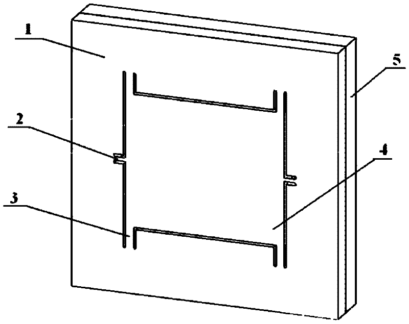
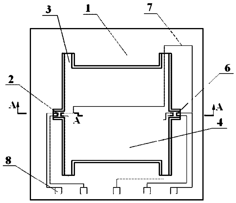
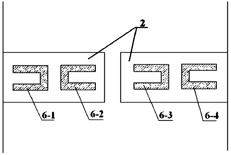
[0028] refer to figure 1 , an acceleration sensor chip with a composite multi-beam structure, comprising a silicon substrate 1, the back of which is bonded to boron glass 5, a suspended mass 4 is arranged in the central cavity of the silicon substrate 1, four identical support beams 3 two Two groups are connected to one set of opposite sides of the suspended mass 4, and two identical sensitive beams 2 are respectively connected to the other set of opposite sides of the suspended mass 4, and the support beam 3 and the sensitive beam 2 jointly support the suspended mass 4, so that It remains in a suspended state, boron glass 5 is bonded to the back of silicon substrate 1, and a working gap is reserved with the bottom surface of suspended mass 4 to ensure that suspended mass 4 can always be suspended in the air when the sensor is working normally, and in some overl...


PUM


Abstract

The invention provides an acceleration sensor chip with a compound multiple-beam structure and a manufacturing method thereof. The acceleration sensor chip is characterized in that: four support beams and two sensitive beams support a hanging mass block, and the hanging mass block is suspended; the sensitive beam is provided with a plurality of voltage dependent resistors which are connected to form a semi-open-loop Wheatstone bridge, and an output terminal of the bridge is connected with pads of a chip. The manufacturing method of the chip comprises the following steps: thinning a hang mass block area silicon chip, and carrying out lithography and sputtering on a right side of the chip to form a metal lead wire and the pads; carrying out lithography at a back side of the silicon chip andwet method etching to form a movable structure composed of the sensitive beam, the support beam, and the hang mass block, bonding boron glass at a back side of a silicon chip substrate, and carrying out right side lithography and etching to form gap between a chip movable part and a silicon substrate to obtain the chip. When ensuring measure sensitivity of the sensor, response frequency of the acceleration sensor is raised, and performance of the sensor in dynamic acceleration measurement is enhanced. The manufacturing method of the chip has the characteristics of simplicity and high reliability, and realization of micromation and low cost is facilitated.

Description

technical field [0001] The invention relates to an acceleration sensor chip, in particular to an acceleration sensor chip with a composite multi-beam structure and a manufacturing method thereof. Background technique [0002] At present, due to the development of MEMS technology, acceleration sensors based on different sensitive principles have been designed and manufactured, and have been widely used. Accelerometers with different sensitivity principles have different advantages and disadvantages. For example, the technology and performance of piezoelectric acceleration sensors have matured and have been widely used in the market. However, due to the limitation of sensitive principles, piezoelectric sensors cannot perceive static acceleration values, and the output is a charge signal, which requires a proprietary follow-up Auxiliary circuit; the capacitive acceleration sensor has high sensitivity, small temperature drift, low power consumption, and good stability, but the ...

Claims


Application Information

Patent Timeline
IPC IPC(8): G01P15/12B81C1/00
Inventor 赵玉龙刘岩孙禄田边蒋庄德
Owner XI AN JIAOTONG UNIV
Why Eureka
Try Eureka