Manufacturing method for reducing hot carrier injection damage of semiconductor device

A hot carrier and injection damage technology, which is applied in semiconductor/solid-state device manufacturing, electrical components, circuits, etc., and can solve the difficulty of PMOS device threshold voltage process line control, PMOS device threshold voltage drift, and boron punch-through aggravation, etc. question

Inactive Publication Date: 2011-12-28
SHANGHAI HUALI MICROELECTRONICS CORP
View PDF2 Cites 4 Cited by
  • Summary
  • Abstract
  • Description
  • Claims
  • Application Information

AI Technical Summary

Problems solved by technology

However, the fluorinated gate oxide layer 104 will bring new problems, because fluorine exists in the overall silicon dioxide gate oxide layer 104, such as Figure 1c As shown, the boron ions 114 in the polysilicon 106 can penetrate into the channel of the MOS device more easily, that is, the boron penetration (Boron Penetration) phenomenon will be aggravated, which will cause the threshold voltage drift of the PMOS device, and the process line control difficulty of the threshold voltage of the PMOS device increase
[0005] In order to solve the above problems and avoid the boron punch-through phenomenon caused by implanting fluorine atoms in the overall gate oxide layer to improve the anti-hot carrier injection performance of MOS devices, in order to improve the life of MOS devices, it is necessary to perform well implantation (Well Implantation) process, light Doped Drain (LDD, Lightly Doped Drain) structure implantation process and other implantation processes are looking for solutions, but there are still considerable barriers in the actual implementation process, and it is urgent to introduce new methods that can effectively improve the above defects to solve MOS. The device can not only effectively prevent the failure of the hot carrier effect, but also effectively suppress the occurrence of boron punch-through phenomenon

Method used


Image

  • Manufacturing method for reducing hot carrier injection damage of semiconductor device
  • Manufacturing method for reducing hot carrier injection damage of semiconductor device
  • Manufacturing method for reducing hot carrier injection damage of semiconductor device

Examples


Embodiment Construction

[0019] In order to make the above objects, features and advantages of the present invention more comprehensible, specific implementations of the present invention will be described in detail below in conjunction with the accompanying drawings.

[0020] In the following description, numerous specific details are set forth in order to provide a thorough understanding of the present invention. However, the present invention can be implemented in many other ways different from those described here, and those skilled in the art can make similar extensions without violating the connotation of the present invention, so the present invention is not limited by the specific implementations disclosed below.

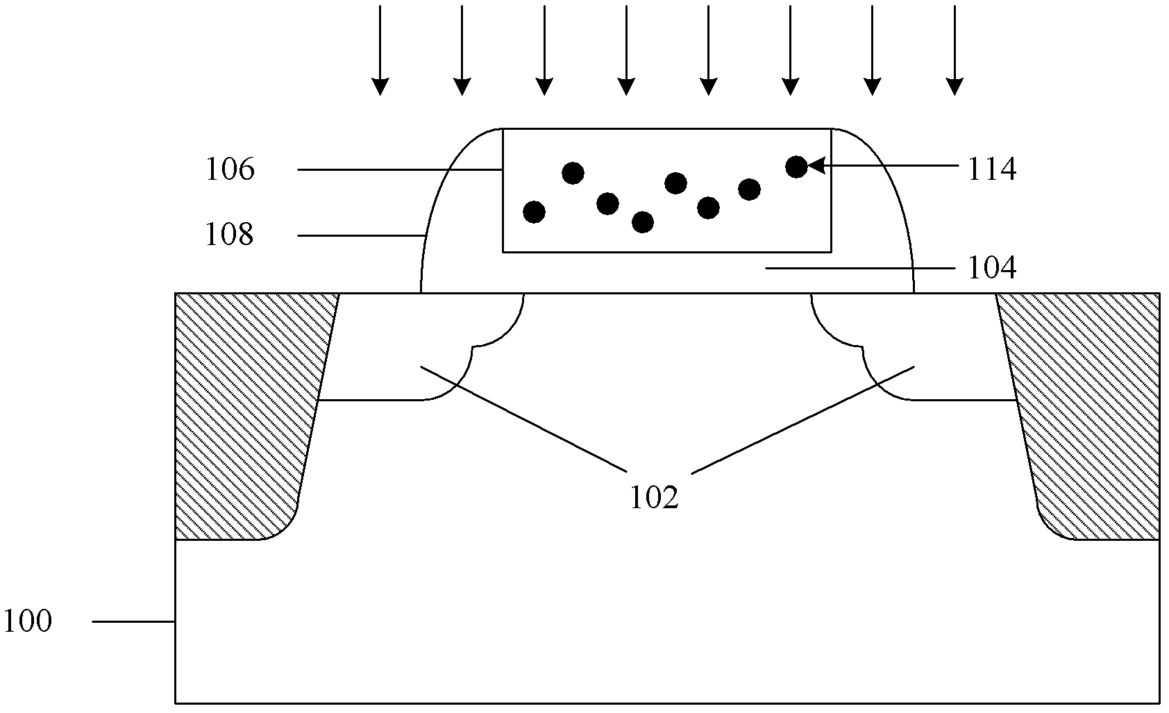
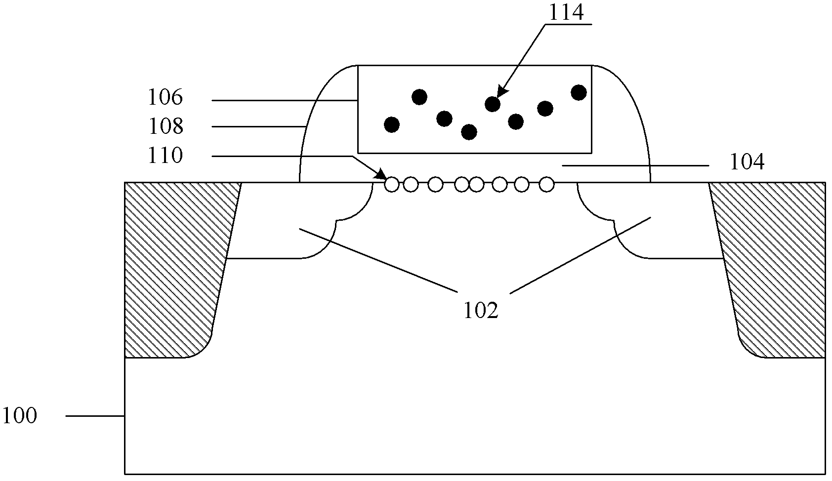
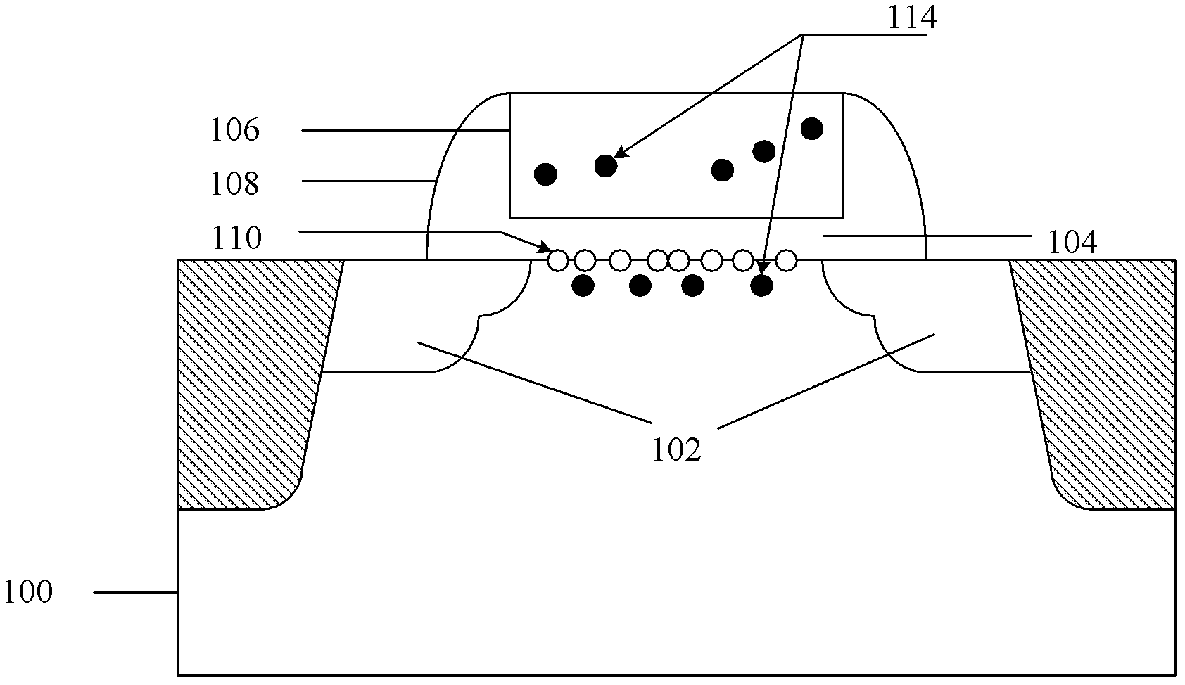
[0021] Secondly, the present invention is described in detail using schematic diagrams. When describing the embodiments of the present invention in detail, for the convenience of explanation, the cross-sectional view showing the device structure will not be partially enlarged accordi...


PUM


Abstract

The invention proposes a manufacturing method for reducing hot carrier injection damage of a semiconductor device, comprising the following steps: forming an n well and a p well in a semiconductor substrate, growing a gate oxide layer above the substrate, and forming a gate oxide layer on the gate oxide layer. Polysilicon gate; after covering the photoresist layer above the n-well region, perform source-drain implantation of lightly doped drain region structure in the p-well region; ash the photoresist layer with a combination gas containing carbon tetrafluoride and source-drain in the p-well region Silicon-fluorine bonds are formed at the end interface; after covering the photoresist layer above the p-well region, the lightly doped drain region structure source-drain implantation is performed on the n-well region; the photoresist layer is ashed with a combination gas containing carbon tetrafluoride and A silicon-fluorine bond is formed at the source-drain interface of the n-well region; gate sidewalls are fabricated and source-drain implants are performed to form source and drain electrodes. The invention provides a manufacturing method of a MOS device capable of reducing the hot carrier injection damage of the semiconductor device, which can not only prevent the hot carrier injection damage of the MOS device, but also suppress the boron punch-through phenomenon.

Description

technical field [0001] The invention relates to a semiconductor preparation technology, in particular to a manufacturing method for reducing hot carrier injection damage of semiconductor devices, which can effectively prevent hot carrier injection damage of MOS devices without causing serious boron punch-through phenomenon . Background technique [0002] As the integration process technology enters the deep submicron process conditions, the power supply voltage and operating voltage of the chip have not decreased a lot correspondingly, so the electric field strength inside the corresponding device increases with the reduction of the device size. In small-sized devices, the lateral size of the circuit is getting smaller and smaller, resulting in a reduction in gate oxide thickness, junction depth, and channel length. Even a small source-drain voltage will form a high electric field strength near the drain terminal. Due to the effect of the transverse electric field, in the s...

Claims


Application Information

Patent Timeline
Patent Type & Authority Applications(China)
IPC IPC(8): H01L21/8238
Inventor 俞柳江李全波黄晓橹
Owner SHANGHAI HUALI MICROELECTRONICS CORP
Why Eureka
Try Eureka