Package structure with antenna and manufacturing method thereof

A technology of packaging structure and manufacturing method, which is applied in semiconductor/solid-state device manufacturing, electrical components, electric solid-state devices, etc., can solve the problems of large antenna circuit board area and high design and manufacturing costs, and achieve reduced area, design and manufacturing costs Effect

Active Publication Date: 2011-12-28
UNIVERSAL SCIENTIFIC INDUSTRIAL (SHANGHAI) CO LTD +1
View PDF5 Cites 25 Cited by
  • Summary
  • Abstract
  • Description
  • Claims
  • Application Information

AI Technical Summary

Problems solved by technology

[0004] The technical problem to be solved by the present invention is to provide a method and structure for making an antenna on the surface of a package, and to provide a method and a structure for making an antenna on the surface of the package simultaneously in order to overcome the defects of the large area of ​​the circuit board occupied by the antenna and the high cost

Method used


Image

  • Package structure with antenna and manufacturing method thereof
  • Package structure with antenna and manufacturing method thereof
  • Package structure with antenna and manufacturing method thereof

Examples


Example

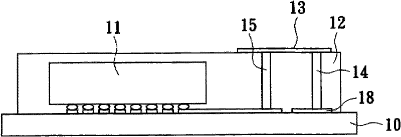
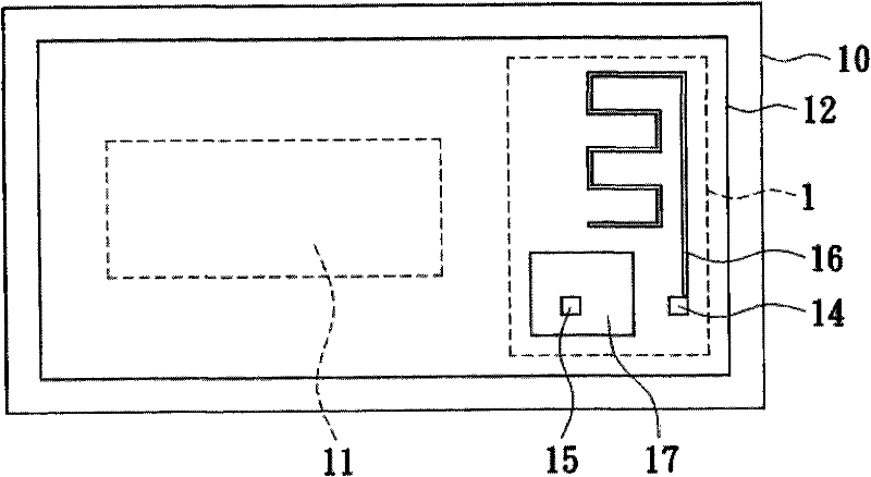
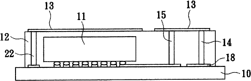
[0048] According to the first embodiment of the present invention, the package body 12 covers the IC chip 11 and the circuit pattern 18, and two through holes 14 (first through holes), 15 are made at a predetermined position of the package body 12 to expose the circuit pattern An antenna signal terminal and a ground terminal of the high-frequency circuit of 18. A conductive metal layer 13 is plated on the surface of the package body 12, which can be achieved by sputtering or other coating methods, and the conductive metal layer 13 can be gold, silver, copper, aluminum, titanium and alloys thereof or It is other conductive materials. Then, the shape of the antenna pattern 16 and the grounding plane 17 are formed on the conductive metal layer 13 using a laser engraving machine or a traditional yellow photolithography process and an etching process. Finally, the through holes 14 and 15 are filled with a coating method to connect the feed end of the antenna signal of the antenna p...


PUM


Abstract

The invention discloses a packaging structure with an antenna and a manufacturing method thereof. The method comprises the following steps of: forming a circuit diagram and an integrated circuit (IC) chip on a substrate, wherein the IC chip is electrically connected with the circuit diagram; covering a package on the substrate to wrap the circuit diagram and the IC chip; and forming an antenna diagram on the package, wherein the antenna diagram is electrically connected with the circuit diagram by using a first through hole passing through the package. Therefore, the antenna can be formed on the package of the circuit board, and the purpose of reducing the area of a circuit board is reduced.

Description

technical field [0001] The invention relates to a method for manufacturing an antenna, in particular to a method for manufacturing an antenna on a packaging body and its structure. Background technique [0002] Due to the advancement of technology, various high-tech electronic products have been developed to facilitate people's life, including various electronic devices, such as notebook computers, mobile phones, personal digital assistants (PDAs), and the like. With the popularization of these high-tech electronic products and the increase of people's demand, in addition to the substantial increase of various functions and applications configured in these high-tech products, especially in order to meet people's mobile needs, the function of wireless communication has been added. Therefore, people can use these high-tech electronic products at any place or at any time through these high-tech electronic devices with wireless communication functions. Thereby greatly increasin...

Claims


Application Information

Patent Timeline
IPC IPC(8): H01L23/66H01L21/60H01L23/552
CPCH01L2223/6677H01L2224/16225H01L23/552H01L2224/16227H01L2924/3025
Inventor 焦嘉振杨超雅蔡宗贤
Owner UNIVERSAL SCIENTIFIC INDUSTRIAL (SHANGHAI) CO LTD
Why Eureka
Try Eureka