
Cell electrofusion chip device based on surface microelectrode array and deformation membrane structure

A technology of microelectrode array and membrane structure, which is applied in the field of biological cell electrofusion, can solve the problems of inability to accurately realize AB cell pairing and fusion, precise control of unfavorable cells between electrodes, and high electrical safety requirements, and achieve good biophase Capacitance and anti-corrosion properties, solving cell pairing, and high fusion efficiency

Inactive Publication Date: 2012-01-04
RES COOPERATION FOUND OF YEUNGNAM UNIV
View PDF5 Cites 5 Cited by
  • Summary
  • Abstract
  • Description
  • Claims
  • Application Information

AI Technical Summary

Problems solved by technology

[0007] However, the traditional cell electrofusion equipment also has some disadvantages: (1) Due to the large electrode spacing in the fusion tank, a high external driving voltage is required to achieve sufficient strength of cell queuing, fusion and compaction signals, often as high as several Hundreds of thousands of volts, high requirements on the electrical safety of the system, the cost of the system is also greatly increased; (2) The large distance between electrodes is not conducive to the precise control of cells, etc.
The cell pairing of the cell electrofusion chip device based on the micro-chamber array structure proposed by the research group is based on a random principle of cell pairing and fusion. Although it can achieve the goal of pairing two cells, it still cannot accurately achieve the pairing of AB cells. and integration (see Chinese patent 200910191052.0)

Method used


Image

  • Cell electrofusion chip device based on surface microelectrode array and deformation membrane structure
  • Cell electrofusion chip device based on surface microelectrode array and deformation membrane structure
  • Cell electrofusion chip device based on surface microelectrode array and deformation membrane structure

Examples


Embodiment Construction

[0040] Below in conjunction with accompanying drawing, further illustrate structure and working method of the present invention:

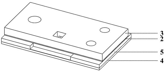
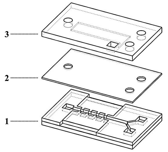
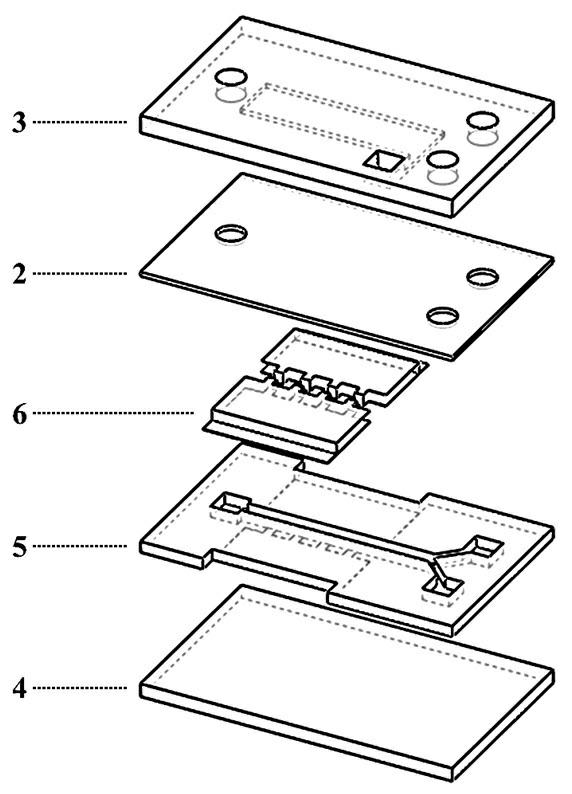
[0041] see figure 1 , figure 2 and image 3 , the cell electrofusion chip device based on the surface body microelectrode array and the deformable membrane structure is composed of the surface body microelectrode array chip 1 and the deformable membrane structure composed of the flexible deformable membrane 2 and the air pressure adjustment device 3 .

[0042] The specific structure of the surface body microelectrode array chip 1 is as follows: on the quartz base layer 4, a bottom layer of comb-shaped microelectrode array 7 is fabricated through a micromachining process, and the bottom comb-shaped microelectrode array 7 is opposite to each other on the quartz base layer 4. Two groups are symmetrically arranged in the form of two groups, and a passage is left between the two groups. The polymer microchannel layer 5 is molded by soft lithography...


PUM


Abstract

The invention relates to a cell electrofusion chip device based on a surface microelectrode array and a deformation membrane structure. The cell electrofusion chip device is composed of a surface microelectrode array chip and a top-layer deformation membrane structure, wherein the surface microelectrode array chip is divided into a quartz base layer, a microelectrode array layer and a polymer microchannel layer; the microelectrode array is in a sandwich structure and is attached to the polymer microchannel layer, thereby avoiding the cell blockage problem caused by the traditional tooth-shaped projection electrode structure and simultaneously guaranteeing the integration level and better fusion efficiency of the microelectrode; the deformation membrane structure is composed of a flexible deformation membrane and an air pressure adjusting device; the flexible deformation membrane covers the microchannel; and the flexible deformation membrane deforms under the action of air pressure applied by the air pressure adjusting device, protrudes downwards and enters the microchannel to form a partition wall, thereby dividing the microchannel into two microchannels and realizing independent feeding and pairing of different cells. The device can be widely applied in the fields of genetics, distant hybridization breeding of animals and plants, developmental biology, drug screening, monoclonal antibody preparation, mammal cloning and the like.

Description

technical field [0001] The invention relates to a device for electrical fusion of biological cells. In particular, the invention relates to chips that provide electrofusion of cells. Background technique [0002] Since the 1980s, cell electrofusion technology has been rapidly developed and widely used because of its advantages such as high efficiency, easy operation, non-toxic to cells, easy observation, suitable for instrument application and standardized operation (see 4326934, April 27, 1982, Pohl; 441972, April 10, 1982, Pohl; 4578168, March 25, 1986, Hofman; 4695547, Sep 22, 1987, Hillard; 4699881, Oct 13, 1987, Matschke, et al. ;). [0003] Cell electrofusion can be divided into two main stages: cell queuing and cell fusion. [0004] The principle of cell queuing is that when biological cells are in a non-uniform electric field, they are polarized by the electric field to form a dipole, and the dipole will move under the action of a specific force under the action o...

Claims


Application Information

Patent Timeline
IPC IPC(8): C12M1/42
CPCC12M25/02C12M35/02C12M23/26
Inventor 胡宁钱诗智朱祥佑
Owner RES COOPERATION FOUND OF YEUNGNAM UNIV
Learn More