Sequentially etched and plated lead frame structure without island prepacked plastic sealed material and producing method thereof

A pre-filled molding compound and lead frame technology, which is applied in the direction of electrical components, electrical solid devices, circuits, etc., can solve the problems of unusable, complicated lead frame production procedures, and increased cost of lead frames, etc., to achieve process cost and quality cost reduction , reduce the risk of misalignment, and reduce the effect of complexity

Active Publication Date: 2012-01-18
JCET GROUP CO LTD
View PDF3 Cites 8 Cited by
  • Summary
  • Abstract
  • Description
  • Claims
  • Application Information

AI Technical Summary

Problems solved by technology

[0004] 1. A layer of high temperature resistant adhesive film is attached to the bottom of the metal lead frame, which increases the cost of the lead frame by at least 50%;
[0005] 2. The adhesive film attached to the bottom of the metal lead frame is a soft organic substance, so in the subsequent packaging process of chip loading and wire bonding operations, volatile pollution of organic substances will be generated due to high-temperature baking, which will directly pollute The bonding between the front of the chip and the front of the lead frame and the wire bonding will even affect the failure of the bonding ability with the plastic encapsulant during the subsequent packaging process between the front of the chip and the front of the lead frame (commonly known as delamination);
[0006] 3. Because the soft organic adhesive film is attached to the bottom of the lead frame, part of the bonding force is absorbed by the soft organic adhesive film during the subsequent wire bonding operation in the packaging process, increasing the wire Difficulty in bonding, resulting in instability of wire bonding yield, which may cause reliability problems;
[0007] 4. Because the soft organic adhesive film is attached to the bottom of the lead frame, the metal wire material is limited to soft and expensive gold wire during bonding, instead of hard and low-cost copper and aluminum. quality or other low-cost wire or strip;
[0009] 6. Usually, QFN products must have a metal base island before they can be mounted. Sometimes it will bring some troubles to the circuit board design, because it is necessary to prevent the short circuit between the line and the metal base island.
[0011] 1. The production process of the lead frame is too complicated, resulting in an increase in the cost of the lead frame;
[0012] 2. The etching of the lead frame is divided into upper and lower etching once, which is easy to cause misalignment due to repeated positioning errors of the upper and lower etching positions

Method used


Image

  • Sequentially etched and plated lead frame structure without island prepacked plastic sealed material and producing method thereof
  • Sequentially etched and plated lead frame structure without island prepacked plastic sealed material and producing method thereof
  • Sequentially etched and plated lead frame structure without island prepacked plastic sealed material and producing method thereof

Examples


Embodiment Construction

[0052] The present invention relates to a baseless island pre-filled plastic encapsulant. The production method is as follows:

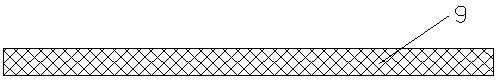
[0053] Step 1. Take the metal substrate

[0054] see figure 1 1. Take a metal substrate 9 with a suitable thickness. The material of the metal substrate 9 can be changed according to the functions and characteristics of the chip, such as copper, aluminum, iron, copper alloy, stainless steel or nickel-iron alloy.

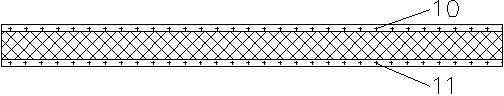
[0055] Step 2, film pasting operation

[0056] see figure 2 , using a film sticking device to paste photoresist films 10 and 11 that can be exposed and developed on the front and back of the metal substrate 9, respectively, to protect the subsequent etching process, the photoresist films 10 and 11 can be dry films, It can also be wet film.

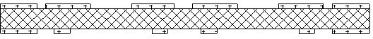
[0057] Step 3. Remove part of the photoresist film on the front and back of the metal substrate

[0058] see image 3 , using the exposure and development equipment to expose, develop and remove...


PUM


Abstract

The invention relates to a sequentially etched and plated lead frame structure without an island prepacked plastic sealed material and a producing method thereof. The structure comprises pins (2), wherein front faces of the pins (2) are plated with first metal layers (5); back faces of the pins (2) are plated with second metal layers (6); etching regions between the pins (2) and the pins (2) are filled with plastic sealed materials (4); and the plastic sealed materials (4) are aligned with the front face and the back face of a metal substrate (9). The sequentially etched and plated lead framestructure provided by the invention has the following advantages: a layer of expensive high temperature resistant soft organic adhesive film needs not to be attached on the bottom of the lead frame; various problems possibly generated in loading, routing and encapsulating are avoided in the background; the yield of the finished products is largely increased; convenience can be brought to the circuit board design while loading is made without a metal island; and the front face and the back face of the lead frame are etched at the same time so that the complicatedness of at least 50% can be reduced in the procedure, the cost is reduced and the malposition risk caused by secondary alignment can be reduced.

Description

technical field [0001] The invention relates to a lead frame structure and a production method thereof, belonging to the technical field of semiconductor packaging. Background technique [0002] There are two main types of traditional lead frame structures: [0003] One is the four-sided flat no-lead package (QFN) lead frame. In order to prevent the lead frame from being sealed on the front side of the lead frame, the back of the lead frame will produce overflow of the plastic packaging compound, so the lead frame is attached to the back of the lead frame. with an expensive high temperature adhesive film (such as Figure 11 shown), this lead frame structure has the following disadvantages: [0004] 1. A layer of high temperature resistant adhesive film is attached to the bottom of the metal lead frame, which increases the cost of the lead frame by at least 50%; [0005] 2. The adhesive film attached to the bottom of the metal lead frame is a soft organic substance, so in t...

Claims


Application Information

Patent Timeline
Patent Type & Authority Applications(China)
IPC IPC(8): H01L23/495H01L21/48
CPCH01L2224/32245H01L2224/85444H01L24/85H01L2224/85464H01L24/73H01L23/49861H01L2224/73265H01L2924/01047H01L24/45H01L2224/45144H01L2224/85439H01L21/4828H01L2224/85455H01L2224/48091H01L2224/97H01L2924/01029H01L24/97H01L2224/48247H01L2224/45124H01L24/32H01L24/48H01L2224/45147H01L2224/48639H01L2224/48644H01L2224/48655H01L2224/48664H01L2224/48739H01L2224/48744H01L2224/48755H01L2224/48764H01L2224/48839H01L2224/48844H01L2224/48855H01L2224/48864H01L2924/181
Inventor 梁志忠谢洁人吴昊耿丛正夏文斌郁科峰
Owner JCET GROUP CO LTD
Why Eureka
Try Eureka