Method for manufacturing semiconductor integrated device

A technology of integrated devices and manufacturing methods, applied in semiconductor/solid-state device manufacturing, electrical components, circuits, etc., can solve the problems of waste of materials, process steps, and low process integration, so as to improve process integration, prevent over-polishing, and save Effect of process steps and consumption of materials

Active Publication Date: 2015-04-01
SHANGHAI HUAHONG GRACE SEMICON MFG CORP
View PDF3 Cites 0 Cited by
  • Summary
  • Abstract
  • Description
  • Claims
  • Application Information

AI Technical Summary

Problems solved by technology

However, since the manufacturing of the split-gate flash memory requires the deposition of a polysilicon layer to form polysilicon word lines, the polysilicon layer in other regions is etched away and then another layer of polysilicon layer is formed to manufacture devices such as MOS transistors and polysilicon resistors, resulting in Waste of material and increase in process steps, low process integration

Method used


Image

  • Method for manufacturing semiconductor integrated device
  • Method for manufacturing semiconductor integrated device
  • Method for manufacturing semiconductor integrated device

Examples


Embodiment Construction

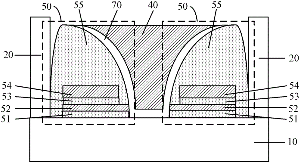
[0030] When forming split-gate flash memory and other semiconductor devices such as MOS transistors, polysilicon resistors, and polysilicon capacitors on the same semiconductor substrate, the manufacturing process of the formed MOS transistors, polysilicon resistors, capacitors and other devices includes the formation of polysilicon layers. The polysilicon layer is etched. If the polysilicon layer deposited in the process of forming the split-gate flash memory is etched away, another layer of polysilicon layer is deposited to form devices such as MOS transistors, polysilicon resistors, and polysilicon capacitors. steps and waste the raw materials for polysilicon deposition.

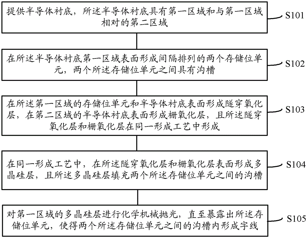
[0031] For this reason, the inventor proposes a kind of semiconductor integrated device manufacturing method through research, please refer to figure 2 ,include:

[0032] Step S101, providing a semiconductor substrate, the semiconductor substrate has a first region and a second region opposite to the fi...


PUM


Abstract

The invention provides a method for manufacturing a semiconductor integrated device, comprising the following steps of: providing a semiconductor substrate; forming two storage bit units on the surface of a first area of the semiconductor substrate in a spaced mode; forming tunneling oxide layers on the two storage bit units in the first area and the surface of the semiconductor substrate and forming gate oxide layers on the surface of the semiconductor substrate in a second area by using the same formation technology; forming polycrystalline silicon layers on surfaces of the tunneling oxide layers and gate oxide layers by using the same formation technology, and filling the polycrystalline silicon layers in the groove between the two storage bit units; and carrying out chemically mechanical polishing on the polycrystalline silicon layer in the first area until the storage bit units are exposed, so that polycrystalline silicon between the two storage bit units forms word lines. In the method, the polycrystalline silicon layers of the polycrystalline silicon word lines formed in a split gate type flash memory are utilized to manufacture other devices with the polycrystalline silicon layers, thus saving the processing steps and the material consumption and improving the processing integrated level.

Description

technical field [0001] The invention relates to semiconductor manufacturing technology, in particular to a method for manufacturing semiconductor integrated devices. Background technique [0002] As the feature size (CD, Critical Dimension) of semiconductor devices becomes smaller and smaller, the integration of semiconductor chips becomes higher and higher, and the number and types of units that need to be formed per unit area are also increasing, so the semiconductor The requirements for craftsmanship are also getting higher and higher. How to rationally arrange the positions of various units and how to save semiconductor process steps and materials by using the common points of each unit manufacturing has become a hot research topic. [0003] In the manufacture of semiconductor devices, polysilicon is a very commonly used conductive material, which can usually be used to make gate electrodes of MOS transistors, high resistance polysilicon resistors, word lines of flash m...

Claims


Application Information

Patent Timeline
Patent Type & Authority Patents(China)
IPC IPC(8): H01L21/8247
Inventor 顾靖孔蔚然于世瑞
Owner SHANGHAI HUAHONG GRACE SEMICON MFG CORP
Why Eureka
Try Eureka