Array substrate, liquid crystal display device as well as manufacturing and repairing method of array substrate

An array substrate and liquid crystal display technology, applied in nonlinear optics, instruments, optics, etc., can solve problems such as electrostatic breakdown of parasitic capacitance and difficult repair, and achieve the effects of improved reliability, easy repair, and flexible setting positions

Inactive Publication Date: 2012-02-01
TCL CHINA STAR OPTOELECTRONICS TECH CO LTD
View PDF4 Cites 20 Cited by
  • Summary
  • Abstract
  • Description
  • Claims
  • Application Information

AI Technical Summary

Problems solved by technology

This technical solution solves the problem of electrostatic breakdown of parasitic capacitance, but there are still some problems. In the array substrate produced by the five-time mask process, the gate line is located at the bottom layer, and there are first insulating layer, data line and second layer on it in sequence. Insulation layer, once the protection capacitor is broken down, it is difficult to repair

Method used


Image

  • Array substrate, liquid crystal display device as well as manufacturing and repairing method of array substrate
  • Array substrate, liquid crystal display device as well as manufacturing and repairing method of array substrate
  • Array substrate, liquid crystal display device as well as manufacturing and repairing method of array substrate

Examples


Embodiment 1

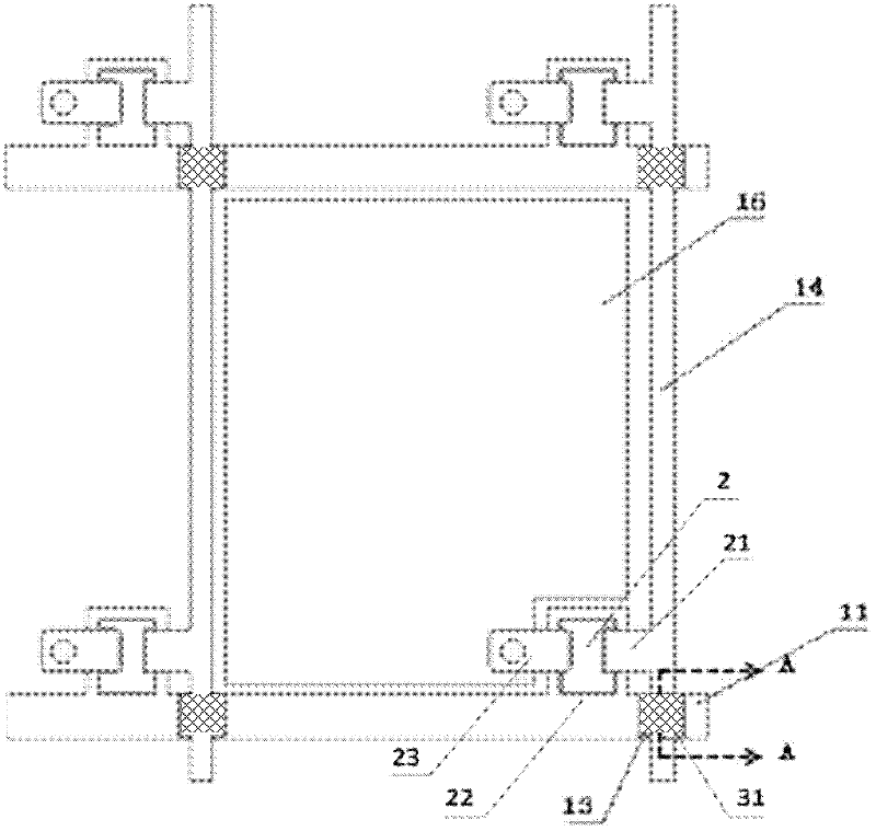
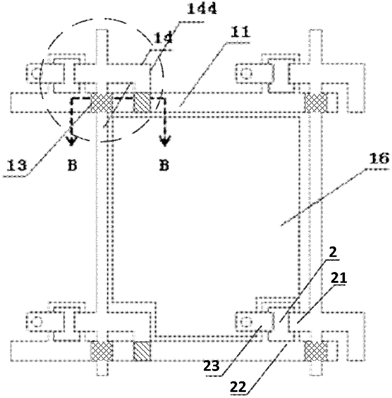
[0033] Embodiment 1, the implementation mode of the thin film transistor liquid crystal display array substrate manufactured based on the five-time mask process of the liquid crystal display device: as Figure 4~6 As shown, the data line of the source electrode 21 of the thin film crystal 2 is extended outward to form a branch portion 144, and the branch portion 144 is bent towards the adjacent gate line 11 until it overlaps with the gate line 11. The overlapping area forms the The protection capacitor 32, that is, the protection capacitor 32 and the parasitic capacitor 31 are formed on the same gate line. Since one end of the parasitic capacitor 31 shares a gate line 11 with the protection capacitor 32, and the other end of the parasitic capacitor 31 communicates with the source 21, that is, communicates with the branch portion 144, the parasitic capacitor 31 and the protection capacitor 32 are electrically connected in parallel. .

[0034] like Figure 5 As shown, the arra...

Embodiment 2

[0046] Embodiment 2, the implementation mode of the thin film transistor liquid crystal display array substrate manufactured based on the four masking process of the liquid crystal display device: as Figure 4 As shown, the data line of the source electrode 21 of the thin film crystal 2 is extended outward to form a branch portion 144, and the branch portion 144 is bent towards the adjacent gate line 11 until it overlaps with the gate line 11. The overlapping area forms the The protection capacitor 32, that is, the protection capacitor 32 and the parasitic capacitor 31 are formed on the same gate line. Since one end of the parasitic capacitor 31 shares a gate line 11 with the protection capacitor 32, and the other end of the parasitic capacitor 31 communicates with the source 21, that is, communicates with the branch portion 144, the parasitic capacitor 31 and the protection capacitor 32 are electrically connected in parallel. .

[0047] like Figure 7 As shown, the array su...


PUM


Abstract

The invention discloses an array substrate, a liquid crystal display device as well as a manufacturing and repairing method of the array substrate. The array substrate of a liquid crystal display with a thin film transistor comprises a pixel electrode, a grid line and a data line, wherein a parasitic capacitor is formed at an overlapping position of the grid line and the data line, the data line is also provided with a branch part overlapped with the grid line to form a protective capacitor connected in parallel with the parasitic capacitor, and the withstand voltage of the protective capacitor is smaller than that of the parasitic capacitor. In the invention, the data line is provided with the branch part overlapped with the grid line to form the protective capacitor which has smaller withstand voltage and is connected in parallel with the parasitic capacitor, and the data line is arranged at a top layer, therefore, it is easier for later repairing.

Description

technical field [0001] The present invention relates to the field of liquid crystal display, and more specifically, relates to an array substrate, a liquid crystal display device and a method for manufacturing and repairing the array substrate. Background technique [0002] Existing technologies such as figure 1 As shown, the liquid crystal display device includes a liquid crystal panel, the liquid crystal panel includes an array substrate, and the column substrate includes a plurality of thin film crystals, a pixel electrode connected to the drain of the thin film crystal, a gate line connected to the gate of the thin film crystal, and a source of the thin film crystal. The data line connected to the electrode; the crossover of the gate and source of the thin film crystal, in the process, the crossover forms a parasitic capacitance. When the charge continues to accumulate, electrostatic discharge (ESD) breakdown is prone to occur and the gate line Short circuit with the da...

Claims


Application Information

Patent Timeline
Patent Type & Authority Applications(China)
IPC IPC(8): G02F1/1362G02F1/1368G02F1/1333G02F1/13
CPCG02F1/1333G02F1/136259G02F1/136286
Inventor 陈虹瑞
Owner TCL CHINA STAR OPTOELECTRONICS TECH CO LTD
Why Eureka
Try Eureka