Method for pre-polishing polishing pad by adopting polysilicon CMP (Chemical Mechanical Polishing) process

A chemical mechanical and pre-grinding technology, which is applied in the direction of grinding devices, grinding machine tools, manufacturing tools, etc., can solve the problems of high production cost, difficulty in reaching the chemical equilibrium state of new grinding pads, and long time required for Poly film production, so as to save time and cost effects

Inactive Publication Date: 2012-02-01
SHANGHAI HUAHONG GRACE SEMICON MFG CORP
View PDF4 Cites 4 Cited by
  • Summary
  • Abstract
  • Description
  • Claims
  • Application Information

AI Technical Summary

Problems solved by technology

Since the grinding surface is silicon dioxide, during the grinding process, the grinding fluid and silicon dioxide cannot Si->Si 4+ chemical reaction, so it is difficult for new polishing pads to reach the required chemical equilibrium

Method used


Image

  • Method for pre-polishing polishing pad by adopting polysilicon CMP (Chemical Mechanical Polishing) process
  • Method for pre-polishing polishing pad by adopting polysilicon CMP (Chemical Mechanical Polishing) process
  • Method for pre-polishing polishing pad by adopting polysilicon CMP (Chemical Mechanical Polishing) process

Examples


Embodiment Construction

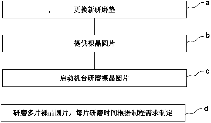
[0016] A kind of specific implementation method of the technical solution of the present invention is provided below in conjunction with accompanying drawing of description,

[0017] Step a, replace the new grinding pad;

[0018] Step b, providing a bare silicon wafer;

[0019] Step c. Start the machine to grind the bare silicon wafer;

[0020] Step d, grinding multiple bare silicon wafers, the grinding time of each piece is determined according to the process requirements)

[0021] In addition, another embodiment provided by the present invention includes the following steps:

[0022] Provide multiple bare silicon wafers;

[0023] Place the wafer boat or wafer boat box (cassette or Pod) containing the bare silicon wafer on the standard mechanical interface (SMIF) of the grinding machine;

[0024] Fix the grinding pad on the grinding mechanical platform, and when the grinding mechanical platform rotates, the grinding pad will rotate synchronously;

[0025] Start the grind...


PUM


Abstract

The invention provides a method for pre-polishing a polishing pad by adopting a polysilicon CMP (Chemical Mechanical Polishing) process. The method not only has the capability of achieving a chemical balance state needed by polishing, but also has low cost and short time. The method provided by the invention is characterized in that: a new polishing pad is pre-polished by adopting a bare wafer; the bare wafer is monocrystalline silicon and can generate a Si<->>Si<4+> chemical reaction with a polishing solution in the pre-polishing process; and a Poly film is not needed to be prepared, therefore the time and cost need by preparation of the Poly film in the traditional scheme are saved.

Description

technical field [0001] The invention relates to the field of semiconductor manufacturing, in particular to a pre-grinding method of polysilicon chemical mechanical polishing (CMP) process. Background technique [0002] In wafer manufacturing, with the upgrading of process technology and the reduction of wire and gate size, lithography technology has higher and higher requirements for the flatness (Non-uniformity) of the wafer surface. The CMP process belongs to chip manufacturing. The basic process of the factory is used to planarize the surface of the wafer. [0003] figure 1 Shown is the schematic diagram of the CMP process equipment. The wafer to be ground is placed under the grinding head (Head) 11. Under the action of downward pressure, the wafer to be ground is mechanically rubbed against the grinding pad (Pad) 13 on the rotating grinding mechanical platform 12. , and realize the grinding under the chemical action of the slurry (Slurry) 14 . According to the differe...

Claims


Application Information

Patent Timeline
IPC IPC(8): H01L21/304B24B37/00
Inventor 李儒兴陈海蓉朱华李志国
Owner SHANGHAI HUAHONG GRACE SEMICON MFG CORP
Why Eureka
Try Eureka