Copper nanowire / copper film composite structure and preparation method thereof

A copper nanowire and composite structure technology, applied in ion implantation plating, metal material coating process, coating, etc., can solve the problems of high substrate requirements, large deposition angle, high cost, etc., and achieve high deposition efficiency, The effect of fast sputtering rate and cost saving

Active Publication Date: 2012-02-08
溧阳常大技术转移中心有限公司
View PDF2 Cites 12 Cited by
  • Summary
  • Abstract
  • Description
  • Claims
  • Application Information

AI Technical Summary

Problems solved by technology

[0003] In the above literature, nanowires prepared by GLAD technology generally have the following characteristics: (1) large deposition angle; (2) high substrate requirements and high cost; (3) nonlinear nanowire morphology; (4) ) The nanowires are short, generally only a few hundred nanometers to a few microns; (5) The nanowires grow perpendicular to the substrate or at a certain angle to the substrate

Method used


Image

  • Copper nanowire / copper film composite structure and preparation method thereof
  • Copper nanowire / copper film composite structure and preparation method thereof
  • Copper nanowire / copper film composite structure and preparation method thereof

Examples


Embodiment 1

[0025] 1) Take an ordinary glass piece and place it in absolute ethanol for ultrasonic cleaning for 8 minutes, then rinse it repeatedly with deionized water for more than 3 times, and then dry the glass piece in an oven at 80°C;

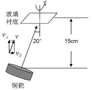
[0026] 2) Fix the prepared glass substrate on the sample tray, install a copper target with a purity of 99.99%, and adjust the copper target to the substrate at 20 ° , adjust the distance between the substrate and the copper target to be 15cm;

[0027] 3) Close the chamber door and vacuum the chamber to 5×10 -4 Pa, the substrate is not heated (about 20°C);

[0028] 4) High-purity Ar gas with a flow rate of 20sccm and a purity of 99.999%, keep the chamber pressure at 0.2Pa, turn on the DC sputtering source, adjust the sputtering power to DC 120W and pre-sputter for 5 minutes to remove possible oxidation on the surface of the copper target Floor;

[0029] 5) No bias was applied to the substrate, the rotation speed of the sample disc was adjusted to...

Embodiment 2

[0032] 1) Same as embodiment 1;

[0033] 2) Same as embodiment 1;

[0034] 3) Raise the substrate temperature to 200°C, and the rest are the same as in Example 1;

[0035] 4) Same as embodiment 1;

[0036] 5) Same as embodiment 1.

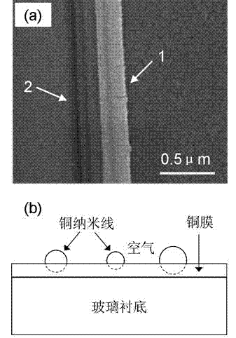
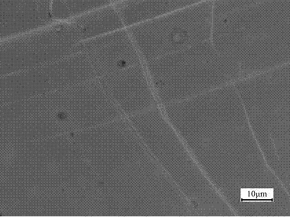
[0037] In the copper nanowire / copper film composite structure prepared in this example, the thickness of the copper film is 57 nm, the length of the copper nanowire is 0.5-4 mm, and the diameter is 100-400 nm. The density of the copper nanowire on the copper film is about 6.7×10 2 / mm 2 .

Embodiment 3

[0039] 1) Same as embodiment 1;

[0040] 2) Same as embodiment 1;

[0041] 3) Same as embodiment 1;

[0042] 4) Same as embodiment 1;

[0043] 5) The thickness of the copper film is 81nm, and the rest are the same as in Embodiment 1.

[0044] In the copper nanowire / copper film composite structure prepared in this example, the thickness of the copper film is 81 nm, the length of the copper nanowire is 0.1-3 mm, and the diameter is 100-450 nm. The density of the copper nanowire on the copper film is about 3.3×10 2 / mm 2 .


PUM

PropertyMeasurementUnit
lengthaaaaaaaaaa
diameteraaaaaaaaaa
thicknessaaaaaaaaaa

Abstract

The invention provides a copper nanowire / copper film composite structure and a preparation method thereof, and aims to provide a copper nanowire / copper film composite structure and a magnetron sputtering preparation method thereof. The invention employs a small deposition angle direct current magnetron sputtering deposition technology and prepares a copper nanowire / copper film composite structure on a glass substrate by proper adjusting of film thickness, substrate temperature and substrate bias voltage. The copper nanowire / copper film composite structure provided by the invention has smooth copper nanowire surface, uniform radial thickness, a length of 0.1-5mm, a diameter of 100-500nm and a copper film thickness of 50-100nm. The copper nanowire is parallel to the copper film surface and embedded in the copper film with a thickness less than that of the copper nanowire. According to the invention, metal copper film surface is embedded with sub-wavelength copper nanowire, which has potential application prospect infields related to surface plasma.

Description

technical field [0001] The invention relates to copper nanowires, and aims to provide a copper nanowire / copper film composite structure and a preparation method thereof by magnetron sputtering and grazing deposition. Background technique [0002] In recent years, vapor deposition technologies such as magnetron sputtering, thermal evaporation, and electron beam evaporation have become more and more widely used, and play a huge role in the fields of industrial production and scientific research; generally, the above vapor deposition methods are mainly used for thin film deposition and surface However, if they are combined with glancing angle deposition (GLAD), it is possible to make nanowires by using the shadowing effect generated during glancing deposition; for example, Karabacak T et al. DC Magnetron Sputtering Grazing Deposition on SiO 2 / Si(100) substrate deposited W nanorods / columns (see literature: 1. Karabacak T, Mallikarjunan A, Singh J P et al, Appl. Phys. Lett., 20...

Claims


Application Information

Patent Timeline
Patent Type & Authority Applications(China)
IPC IPC(8): C23C14/16C23C14/35
Inventor 苏江滨蒋美萍李星星潘丁娟
Owner 溧阳常大技术转移中心有限公司
Why Eureka
Try Eureka