

Semiconductor device and manufacture method thereof
A manufacturing method and semiconductor technology, applied in semiconductor devices, electrical components, circuits, etc., can solve the problems of reducing carrier mobility and unfavorable transistor performance, so as to achieve the effect of optimizing performance and avoiding regrowth
- Summary
- Abstract
- Description
- Claims
- Application Information
AI Technical Summary
Problems solved by technology
Method used
Image

Examples
Embodiment Construction
[0022] The present invention will be further described below in conjunction with specific embodiments and accompanying drawings, but the protection scope of the present invention should not be limited thereby.
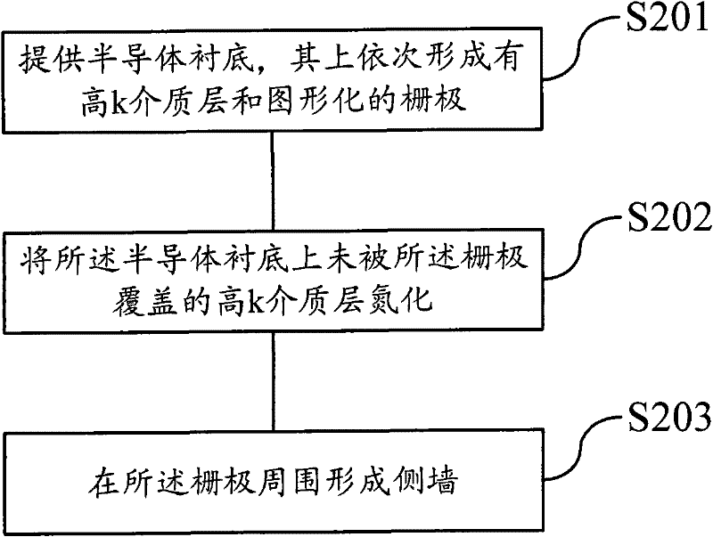
[0023] image 3 It is a schematic flowchart of a method for manufacturing a semiconductor device that suppresses horizontal diffusion of oxygen according to the first embodiment of the present invention. Figure 5 to Figure 8 For the first embodiment of the present invention according to image 3 Schematic diagram of the cross-sectional structure of various stages in the process of manufacturing a semiconductor device that suppresses oxygen horizontal diffusion. Combine below image 3 , 5 -8 Describes the first embodiment of the present invention.
[0024] Such as image 3 , 5 -8, the semiconductor device manufacturing method of the first embodiment of the present invention includes:
[0025] Step S201 , providing a semiconductor substrate 301 on which a high-k ...
PUM
 Abstract
Description
Claims
Application Information