Packaging structure for integrated circuit chip

A technology of integrated circuit and packaging structure, applied in the direction of circuits, electrical components, electric solid devices, etc., can solve problems affecting the normal operation of other electronic products, electromagnetic wave interference of peripheral electronic products, etc., to reduce electromagnetic wave hazards, reduce packaging costs, process Effects that are easy to implement

Inactive Publication Date: 2012-02-08
常熟市广大电器有限公司
View PDF5 Cites 8 Cited by
  • Summary
  • Abstract
  • Description
  • Claims
  • Application Information

AI Technical Summary

Problems solved by technology

The high-frequency chip will release a certain amount of electromagnetic waves during operation, and the electromagnetic waves will be released to the outside through the package, which will easily cause electromagnetic wave interference of peripheral electronic products and affect the normal operation of other electronic products

Method used


Image

  • Packaging structure for integrated circuit chip
  • Packaging structure for integrated circuit chip

Examples


Embodiment Construction

[0018] The preferred embodiments of the present invention will be described in detail below in conjunction with the accompanying drawings, so that the advantages and features of the present invention can be more easily understood by those skilled in the art, so as to define the protection scope of the present invention more clearly.

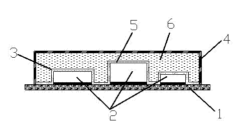
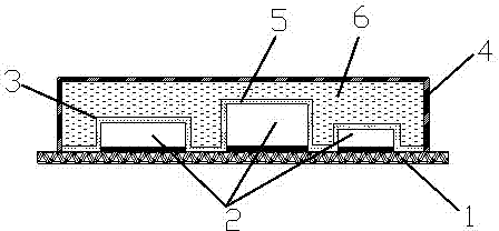
[0019] figure 1 It is a structural schematic diagram of the packaging structure of the integrated circuit chip according to the embodiment of the present invention; the packaging structure of the integrated circuit chip mainly includes a circuit board 1, a chipset 2, a package body 3 and a metal casing 4, and it is characterized in that the chip set 2 Electrically connected to the circuit board 1, and encapsulated by sealing glue, the package body 3 is divided into inner and outer layers, the two layers are prepared with different packaging techniques and materials, and the inner layer package body 5 is closely attached to the Chip set 2, this la...


PUM


Abstract

The invention discloses a packaging structure for an integrated circuit chip. The packaging structure for the integrated circuit chip mainly comprises a circuit board, a chip set, a packaging body and a metal shell. The packaging structure is characterized in that: the chip set is electrically connected with the circuit board and packaged by sealing glue; the packaging body is divided to an internal layer and an external layer; two layers are formed by the different packaging processes and materials; the internal-layer packaging body is adhered to the chip group and formed by a thermally spraying process; the external-layer package body is attached outside the internal-layer package body and made of mixed silicon gel material; and the metal shell is attached outside the package body and electrically connected with the circuit board. In the invention, the packaging structure for the integrated circuit chip is disclosed; the special material and the structure of the packaging body of the packaging structure be used for effectively shielding electromagnetic waves produced by the internal chip and reducing the harm of the electromagnetic waves; and therefore, the common metal shell with a high performance in the market is replaced, the packaging cost is reduced, the process is simply and conveniently implemented and the market prospect is wide.

Description

technical field [0001] The invention relates to a packaging structure of a chip, in particular to a packaging structure of an integrated circuit chip capable of effectively shielding electromagnetic wave radiation and having excellent packaging performance, and belongs to the technical field of chip packaging. Background technique [0002] In the manufacture of integrated circuits, chips are obtained through the steps of wafer fabrication, forming integrated circuits, and cutting wafers. After the integrated circuit of the wafer is fabricated, the chip formed by dicing the wafer can be electrically connected to the carrier outwardly; wherein, the carrier can be a lead frame or a substrate, and the chip can be wire bonded or covered. The method of crystal bonding is electrically connected to the carrier. If the chip and the carrier are electrically connected by wire bonding, then enter into the manufacturing step of filling the encapsulant to form the chip package. Chip pac...

Claims


Application Information

Patent Timeline
Patent Type & Authority Applications(China)
IPC IPC(8): H01L23/552H01L23/29
CPCH01L2224/16225
Inventor 徐子旸
Owner 常熟市广大电器有限公司
Why Eureka
Try Eureka