Method for preparing anti-fingerprint film for touch screen

An anti-fingerprint film and touch screen technology, applied in ion implantation plating, gaseous chemical plating, coating, etc., can solve the problems of high smoothness on the surface of the buffer layer and limit the adhesion of the coating, and achieve the effect of improving the adhesion of the coating

Inactive Publication Date: 2012-02-15
NANCHANG O FILM TECH CO LTD
View PDF3 Cites 20 Cited by
  • Summary
  • Abstract
  • Description
  • Claims
  • Application Information

AI Technical Summary

Problems solved by technology

[0003] Using PECVD to traditional etching, SiO plating 2 Buffer layer and anti-fingerprint film for touch screen three-step process method, SiO coating on the surface of glass substrate 2 When buffer layer and anti-fingerprint film, it is easy to cause SiO 2 The surface smoothness of the buffer layer is extremely high, which limits the SiO 2 Coating adhesion between buffer layer and anti-fingerprint film for touch screen
At the same time, with the development of touch technology, the requirements for the adhesion between the anti-fingerprint film for touch screen and the glass substrate coating are getting higher and higher, and the traditional technology is also facing more and more challenges in terms of coating adhesion requirements.

Method used


Image

  • Method for preparing anti-fingerprint film for touch screen
  • Method for preparing anti-fingerprint film for touch screen
  • Method for preparing anti-fingerprint film for touch screen

Examples


Embodiment Construction

[0020] In order to further illustrate the specific technical content of the invention, the following in conjunction with the embodiments and accompanying drawings describe in detail:

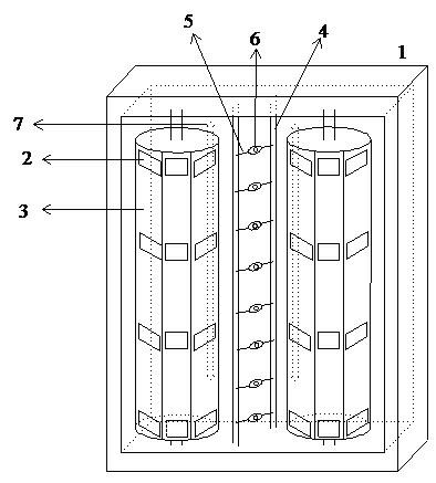
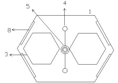
[0021] like figure 1 As shown, in the vacuum chamber 1, the strengthened glass substrate 2 is adhered to the fixture 3, and the filament fixture 4 is clamped with 8 filaments 5, and each of the 8 filaments 5 contains 8 pieces of film material 6, and 7 is a gas pipeline.

[0022] The pressure in the vacuum chamber 1 is pumped to 10 -3 mbar, and then through the gas pipeline 7 to the vacuum chamber 1 into the gas flow rate of 500sccm O 2 and 300sccm Ar to a pressure of 1.0 x 10 -4 ~2.0×10 -2 Between mbar, add intermediate frequency power of 6000w, and then rise to 8000w within 5s to discharge and start for 30s, which can clean and etch the surface of the glass substrate.

[0023] After the etching is completed, the vacuum chamber 1 is evacuated to a pressure of 5.0×10 -3 mbar, then filled wit...


PUM

PropertyMeasurementUnit
thicknessaaaaaaaaaa

Abstract

The invention relates to the technical field of optoelectronic device manufacture, in particular to a preparation method for improving the attachment force of an anti-fingerprint film and a toughened glass substrate in the preparation process of the anti-fingerprint film for a capacitance type touch screen. The preparation method comprises the following steps that: step 1, the clean toughened glass substrate is placed into a plasma enhanced chemical vapor deposition (PECVD) chamber, and the glass substrate is etched and activated through O2 and Ar glow discharge; step 2, SiOx is formed through high-temperature pyrolysis of siloxane, and a SiOx buffer layer is deposited on the surface of the toughened glass substrate after the ion cleaning and the etching; step 3, through the O2 glow discharge, the SiOx buffer layer is etched, the SiOx with poor attachment force is peeled off, O is supplemented, and a SiO2 buffer layer is formed; and step 4, a thermal evaporation method is used for depositing the anti-fingerprint film for the touch screen on the surface of the SiO2 buffer layer formed after the O2 glow discharge.

Description

technical field [0001] The invention is used in the technical field of optoelectronic device manufacturing, and in particular relates to a preparation method for improving the adhesion between the anti-fingerprint film and a strengthened glass substrate in the preparation process of the anti-fingerprint film for a capacitive touch screen. Background technique [0002] Anti-fingerprint and anti-fingerprint films for touch screens have good hydrophobicity and oleophobicity. The permanent topic of the industry. Add a layer of SiO between the anti-fingerprint film for touch screen and glass substrate 2 The buffer layer can improve the coating adhesion between the anti-fingerprint film for the touch screen and the glass substrate. The commonly used methods for preparing the buffer layer and the anti-fingerprint film for touch screen are PVD method and CVD method. Among them, the deposition speed of PVD technology is slow and the adhesion of the coating is insufficient, while th...

Claims


Application Information

Patent Timeline
Patent Type & Authority Applications(China)
IPC IPC(8): C23C16/40C23C16/505C23C14/02
Inventor 熊磊于甄蔡荣军
Owner NANCHANG O FILM TECH CO LTD
Why Eureka
Try Eureka