Wiring structure forming method

A wiring structure and wet etching technology, which is applied in the direction of electrical components, semiconductor/solid-state device manufacturing, circuits, etc., can solve the unfavorable manufacturing cost, the stability of the process quality, the high processing cost of the SOG planarization process, and the control of unfavorable costs etc. to achieve excellent photoelectric properties, improved step morphology, and low film stress

Inactive Publication Date: 2012-02-15
HANGZHOU SILAN INTEGRATED CIRCUIT
View PDF5 Cites 9 Cited by
  • Summary
  • Abstract
  • Description
  • Claims
  • Application Information

AI Technical Summary

Problems solved by technology

[0006] The SOG planarization process, especially the SOG planarization process with glue back engraving, needs to increase the multi-step process steps and corresponding equipment, and the cost of the SOG material used in the SOG planarization process is relatively high, and the storage and application processes are sensitive to temperature and humidity. The stricter requirements lead to higher processing cost of SOG planarization process, and at the same time, it is easy to produce film cracks, SOG moisture absorption, through-hole holes and other process problems, which are not conducive to the control of manufacturing costs and the stability of process quality; Engraving SOG planarization process requires additional expensive equipment while increasing process steps, which is not conducive to cost control

Method used


Image

  • Wiring structure forming method
  • Wiring structure forming method
  • Wiring structure forming method

Examples


Embodiment Construction

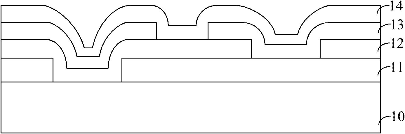
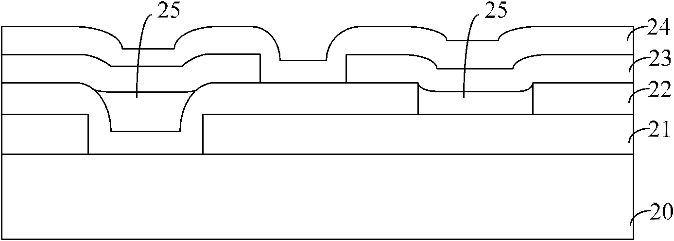
[0032] In the prior art wiring structure formation process, methods such as SOG planarization process are often used to fill the depressions in the front dielectric layer and metal layer, but such methods are relatively complicated and are not conducive to cost control.

[0033] In this embodiment, on the premise of not using the SOG planarization process, the climbing morphology of each film layer is improved by adopting oblique hole contact holes, inverted trapezoidal through-hole structures, and bowl-shaped metal layer openings to meet the step Coverage, step shape and other parameters are also conducive to reducing costs.

[0034]The present invention will be further described below in conjunction with specific embodiments and accompanying drawings, but the protection scope of the present invention should not be limited thereby.

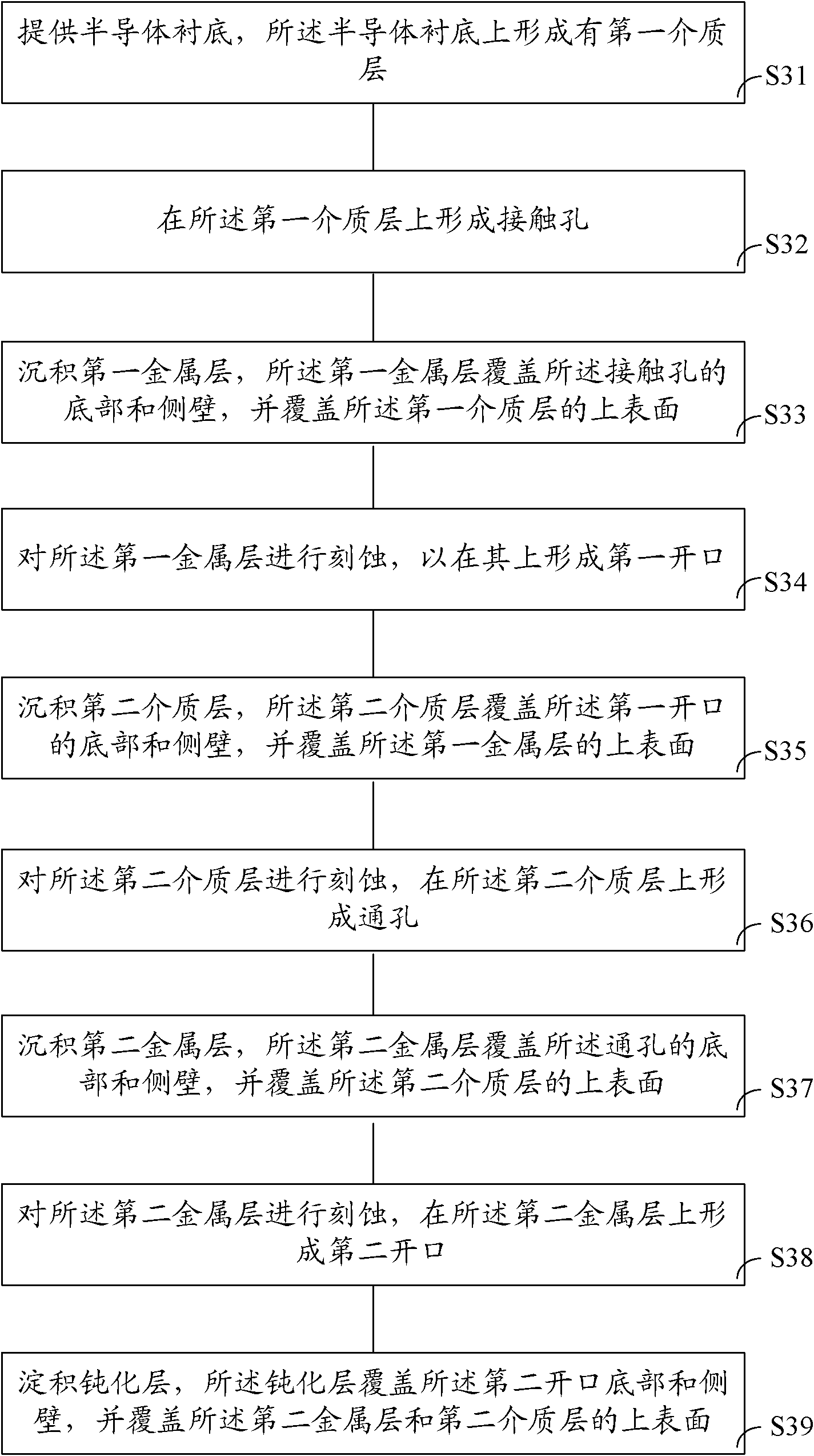
[0035] image 3 A schematic flowchart showing the method for forming the wiring structure of this embodiment, including:

[0036] Step S31, pr...


PUM


Abstract

The invention provides a wiring structure forming method which comprises the following steps of: providing a semiconductor substrate, and forming a first medium layer thereon; forming a contact hole on the first medium layer; depositing a first metal layer, covering the bottom and side wall of the contact hole and covering the upper surface of the first medium layer; etching the first metal layer with a wet method, and etching with a dry method to form a bowl-mouth first opening; depositing a second medium layer, covering the bottom and side wall of the first opening and covering the upper surface of the first metal layer; etching the second medium layer to form an inverted trapezoidal through hole; depositing a second metal layer, covering the bottom and side wall of the through hole and covering the upper surface of the second medium layer; and etching the second metal layer with a wet method, and etching with a dry method to form a bowl-mouth second opening. Through the invention, the requirement on planarization of a process platform of near or below 1.5 microns is met without adopting SOG planarization, glue back-etching SOG planarization and the like.

Description

technical field [0001] The invention relates to the technical field of semiconductor devices and semiconductor technology, in particular to a method for forming a SOG-free wiring structure close to the submicron level (1.5 μm and below). Background technique [0002] In the integrated circuit manufacturing process, SiO is often used 2 and other insulating materials to form a dielectric layer to isolate different metal layers and prevent different metal layers and other conductive layers from penetrating through the conductive layer. The thickness of the dielectric layer is generally 4000 to 10000 Among them, it can be selected according to the requirements of different withstand voltage and parasitic parameters. Due to the relatively thick thickness of the dielectric layer, coupled with the height difference between the opening and the previous metal layer, the step height in some areas is too high, resulting in poor step coverage, process abnormalities, parameter failu...

Claims


Application Information

Patent Timeline
Patent Type & Authority Applications(China)
IPC IPC(8): H01L21/768
Inventor 杨彦涛李小锋冯荣杰罗宁
Owner HANGZHOU SILAN INTEGRATED CIRCUIT
Why Eureka
Try Eureka