Technology mapping method for integrated circuits for improved logic cells

A technology of process mapping and logic unit, applied in the field of process mapping, to achieve the effect of good area, reduced difficulty and excellent performance

Inactive Publication Date: 2012-03-14
AGATE LOGIC BEIJING
View PDF3 Cites 6 Cited by
  • Summary
  • Abstract
  • Description
  • Claims
  • Application Information

AI Technical Summary

Problems solved by technology

[0008] The present invention provides a process mapping method for an integrated circuit of an improved logic...

Method used


Image

  • Technology mapping method for integrated circuits for improved logic cells
  • Technology mapping method for integrated circuits for improved logic cells
  • Technology mapping method for integrated circuits for improved logic cells

Examples


Embodiment Construction

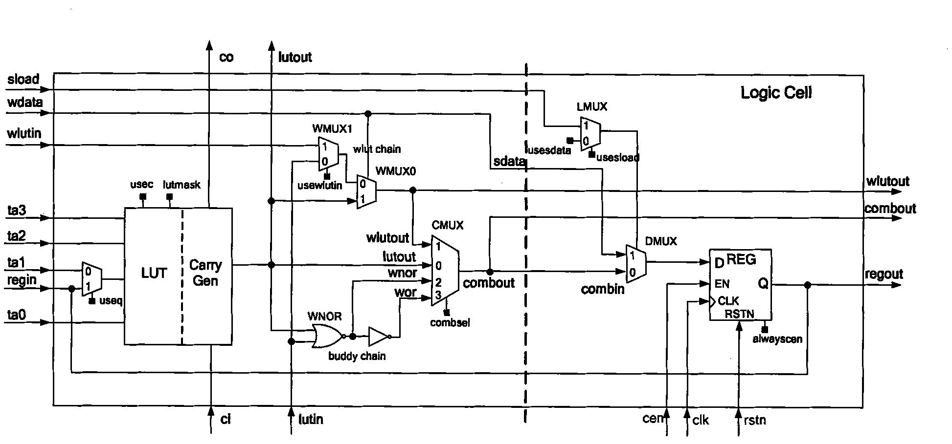
[0034] Figure 10 It is an integrated circuit process mapping flowchart for an improved logic unit according to an embodiment of the present invention.

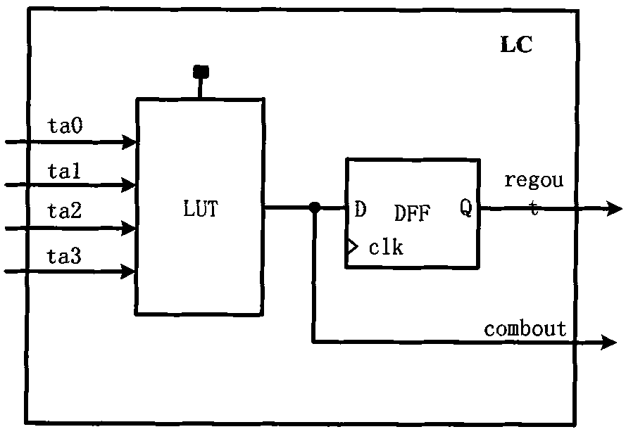
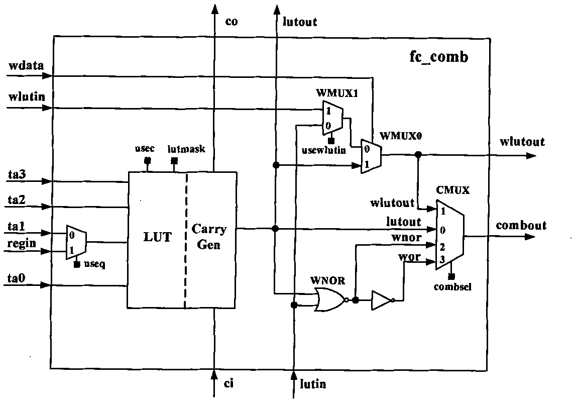
[0035] In an integrated circuit, the circuits in the initial logic netlist are general logic circuits that have nothing to do with physical devices. The general logic circuits include two types, one is general sequential logic circuits, and the other is general combinational logic circuits. Step 101 described below is to map the general sequential logic circuit into a specific function register fc_reg, and steps 102, 103 and 104 are to map the general combinatorial logic circuit into a combinatorial improved logic unit fc_comb. Therefore, step 101 can be before step 102, or after step 104, or anywhere between step 102 and step 104.

[0036] In step 101, according to the initial logic netlist, its general sequential logic circuit is mapped to the corresponding synchronous circuit fc_reg in register form, including mapping int...


PUM


Abstract

The invention relates to a technology mapping method for integrated circuits for improved logic cells, which comprises the following steps of: firstly, decomposing a universal combinational logic circuit into circuits consisting of input logic cells 2; then, taking the input logic cell 2 as a node, partitioning the node based on an improved logic cell, and finding out all partitions of the node; taking a partition corresponding to the maximum ratio of the number of nodes covered by each partition PGCN(Propagate Gate Cover Number) to the number of actually-used improved logic cells PRUN(Propagate Resource Usage Number) as the optimal partition; and finally, converting the optimal partition into a corresponding improved logic cell. By using the method provided by the invention, through fully using the structural advantages of the improved logic cells, an improved circuit is more efficient on area and time. The method provided by the invention can be widely applied to technology mapping of integrated circuits.

Description

technical field [0001] The invention relates to process mapping technology, in particular to a process mapping method for integrated circuits. Background technique [0002] An FPGA (Field Programmable Gate Array, Field Programmable Gate Array) usually includes a large number of logic units. figure 1 A basic FPGA logic cell (logic cell, LC for short) is shown, which includes a look-up table (look-up table, LUT) and a DFF (D flip-flop). The 4-input LUT is shown with a set of configuration memory cells, 16 in total, that can be configured or programmed to compute any 4-input combinational logic function. The output of the LUT is not only directly connected to the output of the LC, but also fed into the D input of the D flip-flop, and the Q output of the D flip-flop can be used as another LC output. Within this logic unit, a multiplexer (MUX) and other logic may be provided to allow the Q output of the flip-flop to be connected to certain inputs of the LUT. [0003] The impro...

Claims


Application Information

Patent Timeline
IPC IPC(8): G06F17/50
Inventor 王海力魏星
Owner AGATE LOGIC BEIJING
Why Eureka
Try Eureka