Evaluation method for failure of contact hole

A technology of failure evaluation and contact hole, which is applied in the direction of color/spectral characteristic measurement, semiconductor/solid-state device testing/measurement, etc. It can solve problems such as missed detection of failed contact holes, difficulty in distinguishing detection machines, and large color difference values. To achieve the effect of avoiding missed or wrong detection

Active Publication Date: 2012-03-14
SEMICON MFG INT (SHANGHAI) CORP +1
View PDF3 Cites 25 Cited by
  • Summary
  • Abstract
  • Description
  • Claims
  • Application Information

AI Technical Summary

Problems solved by technology

[0009] The existing technology has the following problems: the contact hole located in the P-type doped active area is bright when the alignment is normal, and the color difference value is relatively large, but the contact hole located in the N-type doped active area is even The alignment is normal, the scanning brightness is also dark, and the color difference with the surrounding is not obvious
as in figure 2 The area circled by the dotted line in the middle includes several contact holes 13a

Method used


Image

  • Evaluation method for failure of contact hole
  • Evaluation method for failure of contact hole
  • Evaluation method for failure of contact hole

Examples


Embodiment Construction

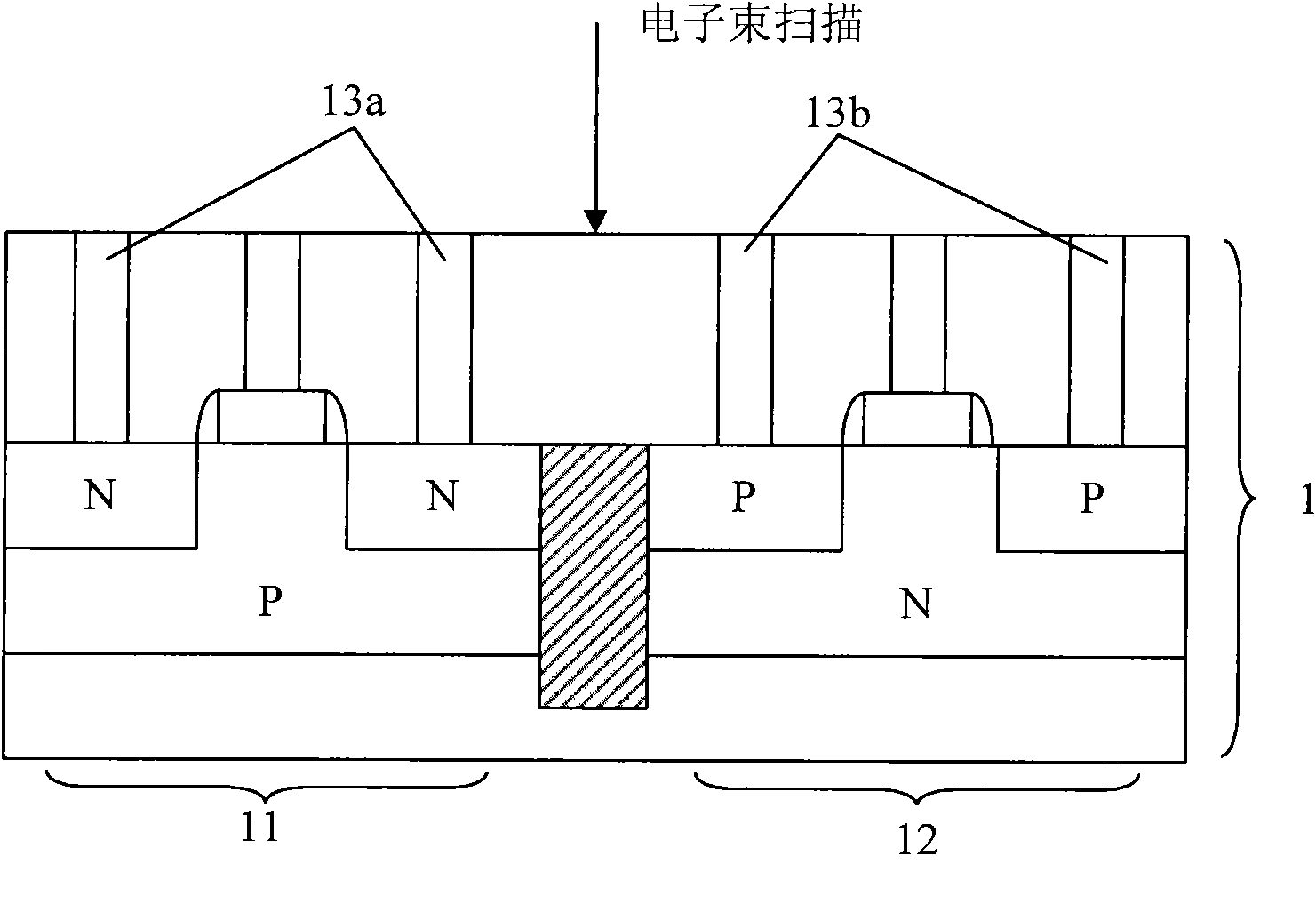
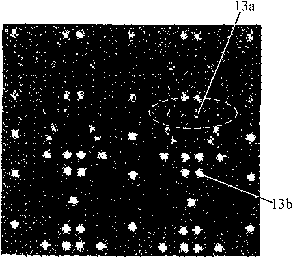
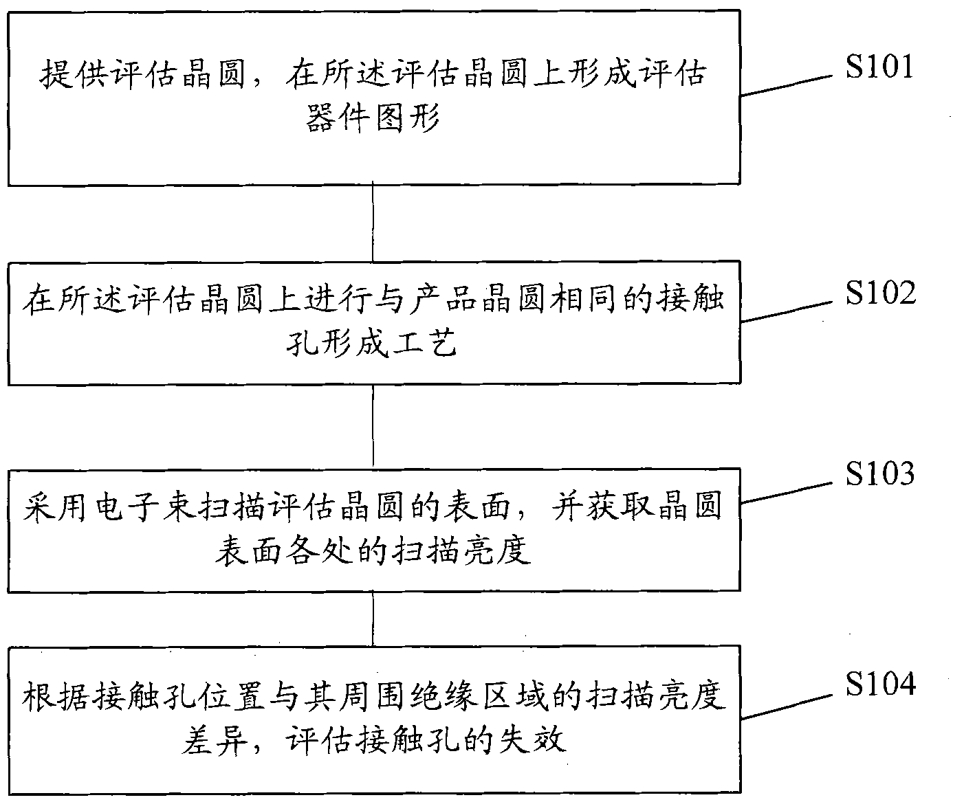
[0030] In the existing contact hole failure evaluation method, the contact hole located on the N-type doped active region shows a gray spot on the color difference diagram when the electron beam is scanned, which is difficult to distinguish from the black of the surrounding insulating region, resulting in mechanical failure. Missed or wrong detection of failed contact holes by the platform. The present invention provides an evaluation wafer having a device pattern similar to the product wafer, so that the N-type or P-type doped active regions on the evaluation wafer have a strong ability to conduct electricity and release charges, so that the electron beam scans at When the contact holes in the above-mentioned active regions are present, they appear as white spots on the color difference diagram, which are easy to distinguish, thereby avoiding the above-mentioned situation of missed detection or wrong detection.

[0031] The present invention will be described in detail below ...


PUM


Abstract

The invention provides an evaluation method for evaluation of a contact hole. The failure evaluation method comprises the following steps of: providing an evaluation wafer and forming an evaluation device graph on the evaluation wafer, wherein the evaluation device graph comprises a first device region and a second device region which has the same structure and size as a PMOS (P-type Metal Oxide Semiconductor) transistor; the difference between the first device region and the NMOS transistor lies in that a P trap corresponding to an NMOS (N-type Metal Oxide Semiconductor) transistor has different doping types, so that the conductivity of an N-type doped active region in the first device region is stronger than a source/drain electrode of the NMOS transistor when the electron beam is scanned; carrying out a forming process of the contact hole which is the same as the product of wafer on the evaluation wafer; and scanning the surface of the evaluation wafer by adopting the electron beamand acquiring the scanning brightness at each part of the wafer surface. According to the evaluation method disclosed by the invention, a brighter light spot is formed when the contact hole is scanned by using the electron beam, thereby the brighter light spot is easily distinguished from a surrounding region and the leakage detection or mistaken detection of the failure contact hole caused by a machine board is effectively avoided.

Description

technical field [0001] The invention relates to the technical field of semiconductor manufacturing, in particular to a contact hole failure evaluation method. Background technique [0002] In the semiconductor manufacturing process, after forming semiconductor devices on the wafer, making contact holes is an important step for metal interconnection. It is necessary to form a corresponding mask for etching the contact hole corresponding to the position of the active region. Wherein, whether the contact hole is aligned with the active area will directly affect the quality of the contact hole. If the formed contact hole cannot be accurately aligned with the bottom active area, the contact hole will fail. Therefore, the contact hole formation process needs to be evaluated before mass production. [0003] The existing contact hole failure evaluation mainly adopts the electron beam color difference method, that is, using the voltage contrast image (Voltage Contrast, VC) technolo...

Claims


Application Information

Patent Timeline
IPC IPC(8): H01L21/66G01N21/25
Inventor 韩秋华黄敬勇宁超
Owner SEMICON MFG INT (SHANGHAI) CORP
Why Eureka
Try Eureka