Through silicon hole structure with step and manufacture process of through silicon hole

A preparation process and technology of through-silicon vias, which are applied in semiconductor/solid-state device manufacturing, semiconductor/solid-state device components, semiconductor devices, etc., can solve problems such as different protrusion heights, different plating rates, and scrapped silicon wafers

Inactive Publication Date: 2012-03-14
HUAZHONG UNIV OF SCI & TECH
View PDF3 Cites 20 Cited by
  • Summary
  • Abstract
  • Description
  • Claims
  • Application Information

AI Technical Summary

Problems solved by technology

Due to the difference in the tiny structure in the through hole, the difference in the internal structure after the electroplating narrows the opening, and the difference in the electroplating process itself, the electroplating rate will be different, and it is very likely that the protrusion height will be different after electroplating. This problem will be resolved in the chemical industry. Stress concentration caused by mechanical polishing (CMP) and bonding process leads to cracking of the silicon wafer and scraps the entire silicon wafer

Method used


Image

  • Through silicon hole structure with step and manufacture process of through silicon hole
  • Through silicon hole structure with step and manufacture process of through silicon hole
  • Through silicon hole structure with step and manufacture process of through silicon hole

Examples


Embodiment Construction

[0026] A typical method of carrying out the invention will now be described with reference to the accompanying drawings.

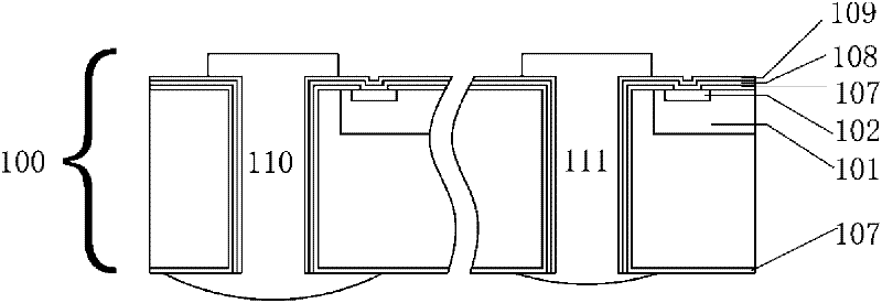
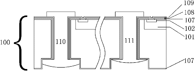
[0027] Such as figure 2 As shown, the structure includes a semiconductor silicon substrate 100 with an integrated circuit 101 (details not shown), integrated circuit pads 102, and two TSV structures formed in the substrate 100 with steps. The TSV structure includes an insulating layer SiO2 107 deposited on the sidewall of the via, a Ti adhesion barrier layer 108 , a copper seed layer 109 , and filling metal copper 110 , 111 . Portions of the copper seed layer 109 on the upper surface of the substrate 100 also serve as lateral interconnects connecting the integrated circuit pads 102 to the fill metal 110 . The copper seed metal layer 109 on the upper surface of the substrate 100 is well bonded to the insulating layer 107 on the substrate through the adhesion barrier layer 108 .

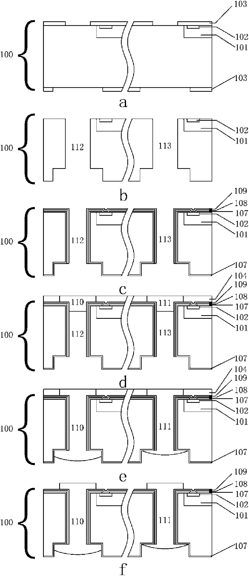
[0028] image 3 A schematic diagram of a typical method for fabricating th...


PUM

PropertyMeasurementUnit
thicknessaaaaaaaaaa
thicknessaaaaaaaaaa

Abstract

The invention discloses a through silicon hole structure with a step, which comprises a semiconductor substrate and a through hole penetrating through the semiconductor substrate and having the step, wherein an insulation layer, an adhesion layer and a barrier layer are sequentially deposited on the side wall of the step through hole; a metal conductor is filled in the through hole; an interconnecting structure formed by sequential deposition of the insulation layer, the adhesion layer, the barrier layer and a conductive layer is deposited on the surface of the semiconductor substrate; and the conductive layer in the interconnecting structure is connected with the metal conductor. The invention also provides a manufacture process of the through silicon hole structure. The step in the through silicon hole can allow copper cylinder protruding height difference caused by local electroplating rate difference in an electroplating hole-filling process, and avoids silicon wafer breakage caused by the problem in a chemical mechanical polishing (MCP) process and a bonding process.

Description

technical field [0001] The invention relates to the technical field of semiconductors, in particular to a through-silicon hole structure in a vertical interconnection structure in a three-dimensional system-in-package and a preparation process thereof. Background technique [0002] At the beginning of the development of the integrated circuit industry, people have continuously reduced the key dimensions and continuously improved the integration of chips to obtain high-performance semiconductor chips. When the critical dimension reaches a few nanometers, continuing to reduce the critical dimension has brought many problems such as a sharp increase in the implementation cost of the lithography process and limitations in the physical properties of the material. [0003] Compared with the existing three-dimensional stack package formed by interconnecting the chip edge leads, through-silicon via technology will bring a three-dimensional package with higher transmission speed, sho...

Claims


Application Information

Patent Timeline
Patent Type & Authority Applications(China)
IPC IPC(8): H01L23/538H01L21/768
Inventor 汪学方王宇哲徐明海徐春林胡畅张卓刘胜
Owner HUAZHONG UNIV OF SCI & TECH
Why Eureka
Try Eureka