General band gap reference starting circuit

A technology for starting circuits and reference circuits, which is applied in the direction of adjusting electrical variables, control/regulating systems, instruments, etc., and can solve the problem of multiple degenerate points of current mode bandgap reference circuits, lack of versatility and practicability, and complex circuit structure. question

Active Publication Date: 2012-03-21
杭州中科微电子有限公司
View PDF5 Cites 29 Cited by
  • Summary
  • Abstract
  • Description
  • Claims
  • Application Information

AI Technical Summary

Problems solved by technology

The prior art U.S. Patent No. US 6489835B1, the patent name is "Low Voltage BandgapReference Circuit", in order to avoid the problem of multiple degeneracy points of the current-mode bandgap reference circuit, the circuit structure is changed to a voltage / current-mode hybrid structure, not only the circuit The structure is complex, and there are defects in sacrificing temperature characteristics and resistance to process angle changes
Another example is the paper "A Low Voltage and LowPower CMOS Bandgap Voltage Reference Design with a Novel Start-up Circuit" published in "Chinese Journal of Semiconductors", 2005, 26 (10) by Xu Changxi et al. The start-up circuit, which introduces a comparator or an operational amplifier, and replicates the technical idea of ​​a parasitic triode, which is highly complex to implement, and the non-ideal factors of the circuit will have a direct impact on the start-up function, so it is not universal and practical

Method used


Image

  • General band gap reference starting circuit
  • General band gap reference starting circuit
  • General band gap reference starting circuit

Examples


no. 1 example

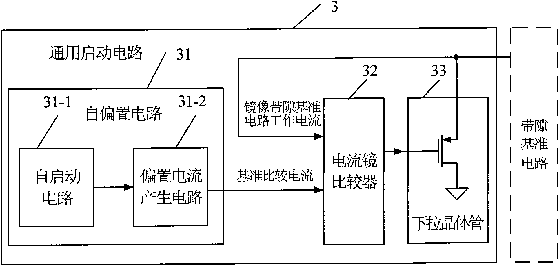
[0054] Figure 4 An electrical schematic diagram of the general bandgap reference starting circuit structure of the first embodiment of the present invention is given. The start-up circuit 4 is composed of a self-bias circuit 41, a current mirror comparator 42 and its pull-down transistor 43 connected in sequence. The self-bias circuit 41 includes a self-start circuit 41-1 and a bias current generating circuit 41-2.

[0055] The self-starting circuit 41 - 1 of the self-bias circuit is composed of NMOS transistors 401 and 402 and a PMOS transistor 406 . The PMOS tube 406 of the self-starting circuit is a PMOS capacitor tube. The drain and source of the PMOS capacitor tube 406 are the upper plate connected to the power supply, and the gate is the lower plate connected to the drain of the NMOS transistor 401 and the gate of the self-bias circuit 402 . The source of the NMOS transistor 401 and the gate of the NMOS transistor 402 of the self-starting circuit are connected to the ...


PUM


Abstract

The invention discloses a general band gap reference starting circuit, which is a current comparison structure and composed of a self-biasing circuit, a current mirror comparison circuit and a pull-down transistor. When used for a voltage mold band gap reference starting circuit, reference currents only need to meet a certain range, the circuit is simple in structure. When used for a current moldband gap reference circuit, the band gap reference circuit works in a wrong working state due to multiple degeneracy points, a current comparison result quickly starts up the starting circuit and enables the band gap reference circuit to be in a normal working state. Simultaneously, a new current comparison result immediately opens the starting circuit, and the reference circuit is not influenced. The starting circuit has good adaptation to working voltage, is not influenced by power voltage change including transient fluctuations and less influenced by process angles, and a circuit structureis simple, thereby being easy to achieve. The general band gap reference starting circuit effectively solves the starting problem of the band gap reference circuits of the two modes and is generally applied to the band gap reference circuit structure under complementary metal oxide semiconductors (CMOS) process.

Description

technical field [0001] The invention belongs to the technical field of digital communication, and relates to a starting circuit of a bandgap reference, in particular to a general-purpose starting circuit of a bandgap reference, which is commonly used in the starting circuit of a current-mode and voltage-mode bandgap reference of a CMOS process, and is especially suitable for low-voltage application. Background technique [0002] In the field of digital communication technology, the bandgap reference circuit is an essential unit module in analog circuits, which provides other circuits with a reference voltage that does not change with temperature and power supply voltage, or a reference current obtained by converting the reference voltage. The bandgap reference circuit has two realization forms of voltage mode and current mode. The typical structure of the bandgap reference circuit of voltage mode is as follows: figure 1 As shown, the typical structure of the current mode ba...

Claims


Application Information

Patent Timeline
Patent Type & Authority Applications(China)
IPC IPC(8): G05F1/56
Inventor 黄伟马成炎叶甜春
Owner 杭州中科微电子有限公司
Why Eureka
Try Eureka