
Patsnap Eureka
For R&D, Patsnap Eureka makes reading and utilizing patents & technical documents easy.
Patsnap Eureka AIR
Designed for self-driven R&D workflows. Generate viable solutions, solve complex R&D challenges, empower your innovation with AI.

Patsnap Eureka Materials
Designed for material experts only. Revolutionize your material R&D, from search, analyze, to developing new materials.

TechResearch
Generate reliable direction feasibility study reports for your R&D in just a few steps.

TechSeek
Discover and master advanced knowledge NOW. Basics, ideas, possibilities, all at once.

TechMind
As an expert in R&D Theories, TechMind can generates customized viable solutions instantly.

TechRisk
Analyze your overall solution with one click, know your potential R&D risks in advance.

TechMonitor
Get weekly tech updates, stay abreast of the latest tech innovations and key insights.
Clamp circuit and flash electro-erasable memory
A clamping circuit, write memory technology, applied in static memory, read-only memory, information storage and other directions, can solve problems such as disadvantage, complicated circuit, simplified process, etc., to achieve stable operation, reduce temperature effect, reduce consumption effect Effect
- Summary
- Abstract
- Description
- Claims
- Application Information
AI Technical Summary
Problems solved by technology
Method used
Image

Examples
Embodiment Construction
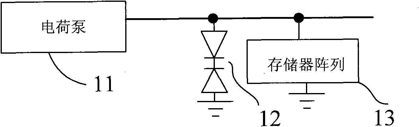
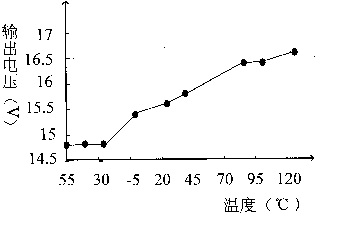
[0032] figure 1 Shown is a schematic structural diagram of an existing flash electric erasable memory circuit, and the output voltage of the charge pump is not less than the clamping voltage of the clamping circuit. When the charge pump outputs a voltage to the clamping circuit, an electric field will be generated at both ends of the clamping circuit. Under the action of the electric field, the first diode is turned on, the second diode is broken down, and the output voltage of the clamping circuit It is equal to the breakdown voltage of the second diode, but the breakdown voltage of the second diode is seriously affected by temperature, and cannot provide a safe and stable working voltage for the memory array within the working temperature range.
[0033] The inventors of the present invention have found that under the action of an electric field, electrons in the second diode migrate from the p region to the barrier region, and holes migrate from the n region to the p region...
PUM
 Abstract
Description
Claims
Application Information
 - R&D Engineer
- R&D Manager
- IP Professional
- Industry Leading Data Capabilities
- Powerful AI technology
- Patent DNA Extraction
Browse by: Latest US Patents, China's latest patents, Technical Efficacy Thesaurus, Application Domain, Technology Topic, Popular Technical Reports.
© 2024 PatSnap. All rights reserved.Legal|Privacy policy|Modern Slavery Act Transparency Statement|Sitemap|About US| Contact US: help@patsnap.com