Crystal silicon solar battery dry etching clamp

A solar cell and dry etching technology, which is applied in the direction of circuits, electrical components, sustainable manufacturing/processing, etc., can solve the problems of uneven application of force at two points, uneven force, easy deformation, etc.

Inactive Publication Date: 2012-03-28
XINYU GIGA SOLAR NEW ENERGY
View PDF5 Cites 2 Cited by
  • Summary
  • Abstract
  • Description
  • Claims
  • Application Information

AI Technical Summary

Problems solved by technology

[0007] a) The force application method in the prior art is two-point force application, and the two-point force application may be uneven, as well as the uneven force on the surface of the silicon wafer, which affects the clamping effect of the edge of the silicon wafer;
[0008] b) The force-bearing sur

Method used


Image

  • Crystal silicon solar battery dry etching clamp
  • Crystal silicon solar battery dry etching clamp
  • Crystal silicon solar battery dry etching clamp

Examples


Embodiment

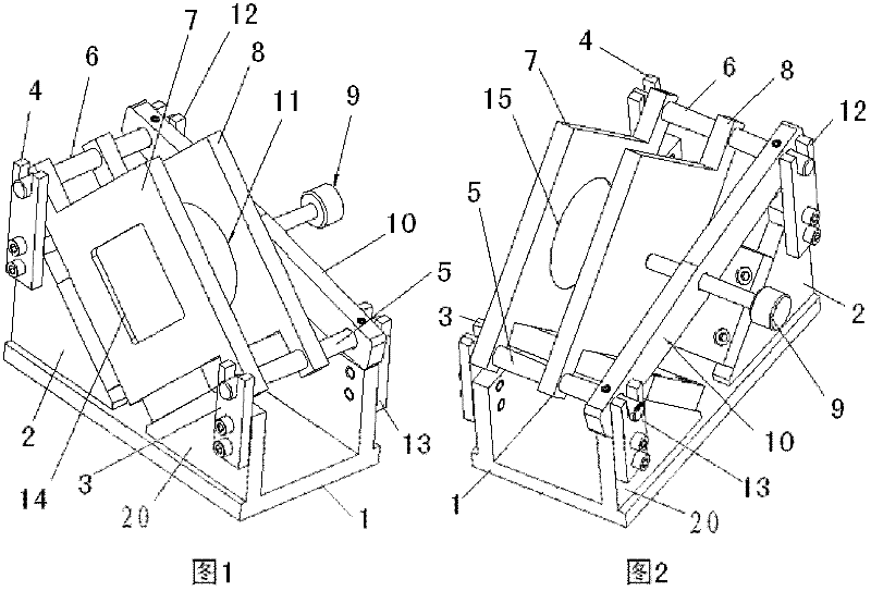
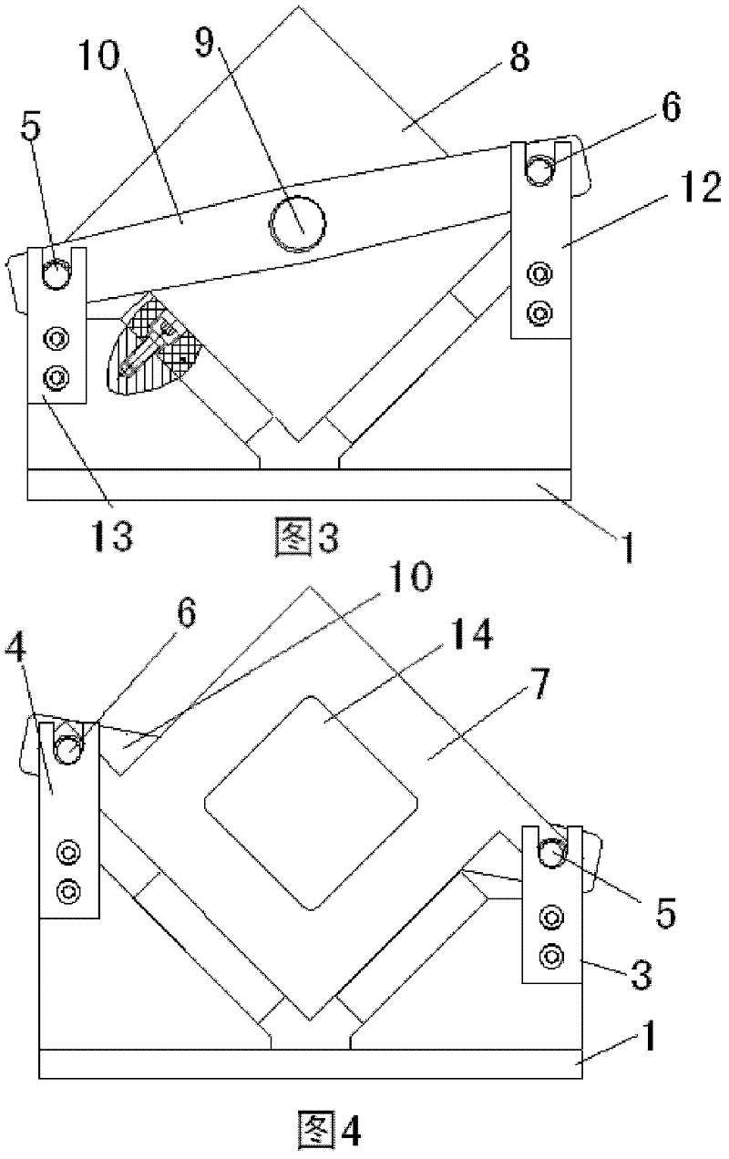
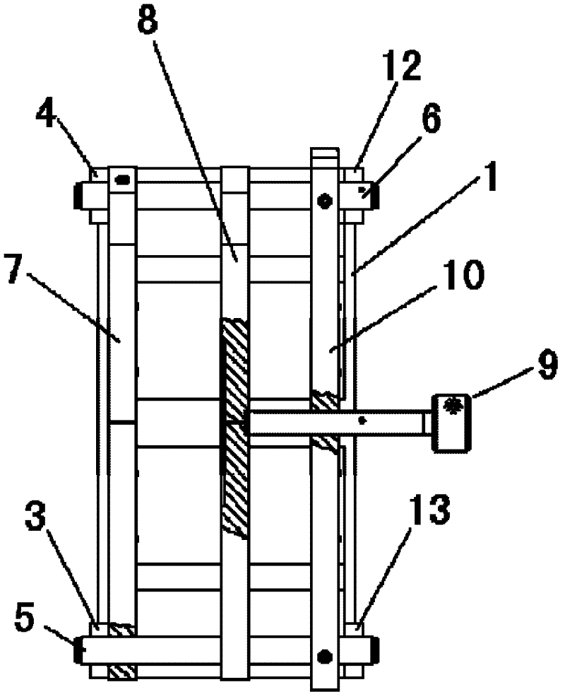
[0042] The present invention provides a fixture for dry etching of crystalline silicon solar cells, which includes a fixed splint 7, a movable splint 8, a screw 9, a silicon chip stacking base 2, a bottom plate 1, a first support seat 3, a second support seat 4, The third support seat 12, the fourth support seat 13, the ejector rod 9, the ejector rod support 10, the first support shaft 5, and the second support shaft 6;

[0043] The bottom plate 1 is connected to the silicon wafer stacking base 2; the two side walls of the first silicon wafer stacking base 2 are fixedly connected with the first supporting base 3 and the fourth supporting base 13 by bolts respectively; the two sides of the second silicon wafer stacking base 20 On the side wall, the third support seat 12 and the second support seat 4 are fixedly connected by bolts respectively; the upper ends of the first support seat 3, the second support seat 4, the third support seat 12 and the fourth support seat 13 have gaps...


PUM


Abstract

A crystal silicon solar battery dry etching clamp belongs to the technical field of solar batteries and adopts the structure that a base plate is connected with a silicon chip stacked base; a first support seat and a fourth support seat are respectively fixed on the two side walls of the silicon chip stacked base through bolts; both a fixed clamp plate and a movable clamp plate are rectangular plates and connected with a first support shaft and a second support shaft respectively, and holes are formed on the opposite angles of the rectangular plates; a central round groove is formed on the inner side contact surface of the fixed clamp plate, and center square groove is formed on the outer side surface of the fixed clamp plate; a center groove is formed on the inner side contact surface of the movable clamp plate; and a bolt rod of an ejector rod is in threaded connection with a ejector rod support, and the top end of the ejector rod is in contact with the movable clamp plate. Due to the above structure, the clamp plate deformation and the uneven stress on the silicon chip caused by force applied to one point are avoided; and a contact surface center chamfer allows the force to bedispersed on the edges of the silicon chips and enables the silicon chip edges to be clamped tightly so as to reduce the stress on the middle areas of the silicon chips. Therefore, the possibility for the etching gas to permeate into the stacked silicon chips is reduced to the maximum degree, and the fragments are reduced; and the silicon chip stacked base allows the stack of the silicon chips tobe more concise, and the fraction between the silicon chips is reduced.

Description

technical field [0001] The invention relates to a fixture for dry etching of crystalline silicon solar cells, belonging to the technical field of crystalline silicon solar cells. Background technique [0002] The meaning of crystalline silicon solar cell is: a power generation device that uses crystalline silicon as a material to convert light energy into electrical energy. [0003] Dry etching means: using gaseous reactants to perform reactive etching on the edge of the silicon wafer. [0004] Facing the global energy crisis, solar photovoltaic power generation technology has become a new development hotspot in the semiconductor industry. The manufacture of crystalline silicon solar cells is divided into processes such as texturing, diffusion, plasma etching, PSG cleaning, PECVD coating, screen printing, and sintering. The diffusion process will cause n-type junction layers to appear on the edge of the silicon wafer, which will cause the positive and negative electrodes of...

Claims


Application Information

Patent Timeline
IPC IPC(8): H01L31/18H01L21/687
CPCY02P70/50
Inventor 孙良欣全成胡盛华俞建范圣凯
Owner XINYU GIGA SOLAR NEW ENERGY
Why Eureka
Try Eureka